CD4047 Datasheet PDF – Monostable Multivibrator – TI

Part Number: CD4047, CD4047B, CD4047BE

Function: CMOS LOW-POWER MONOSTABLE / ASTABLE MULTIVIBRATOR

Package: DIP 14 Pin Type

Manufacturer: Texas Instruments

Image
CD4047 image

Description

The CD4047 consists of a gatable astable multivibrator with logic techniques incorporated to permit positive or negative edge-triggered monostable multivibrator action with retriggering and external counting options. Inputs include +TRIGGER, -TRIGGER, ASTABLE, ASTABLE\, RETRIGGER, and EXTERNAL RESET. Buffered outputs are Q\, Q and OSCILLATOR. In all modes of operation, and external capacitor must be connected between C-Timing and RC-Common terminal, and an external resistor must be connected between the R-Timing and RC-Common terminals.

Pinout

CD4047 datasheet

Features

1. Lower power consumption: special CMOS oscillator configuration

2. Monostable (one-shot) or astable (free-running) operation

3. True and complemented buffered outputs

4. Only one external R anc C required

5. Buffered inputs

6. 100% tested for quiescent current at 20 V

7. Standardized, symmetrical output characteristics

8. 5-V, 10-V, and 15-V parametric ratings

Block Diagram :

CD4047 logic block diagram

Official Homepage: https://www.ti.com/product/CD4047B

CD4047 Datasheet PDF

CD4047 pdf


74HC123 Datasheet PDF – CD74HC123PWT PDF – TI

Part Number: 74HC123, CD74HC123PWT

Function: High-Speed CMOS Logic Dual Retriggerable Monostable Multivibrators with Resets

Package: DIP, SOIC 16 Pin Type

Manufacturer: Texas Instruments

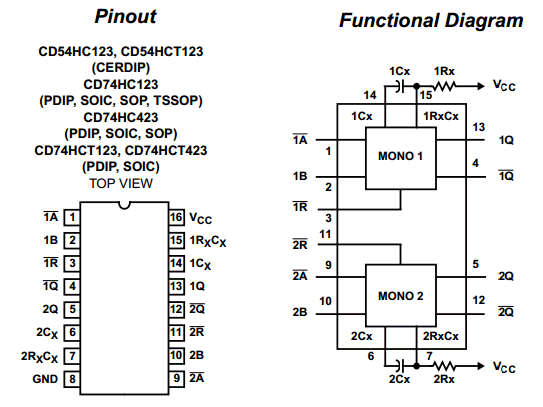
Pinout

74HC123 Pinout ti

Description

The 74HC123, 74HCT123, CD74HC423 and CD74HCT423 are dual monostable multivibrators with resets. They are all retriggerable and differ only in that the 123 types can be triggered by a negative to positive reset pulse; whereas the 423 types do not have this feature. An external resistor (RX) and an external capacitor (CX) control the timing and the accuracy for the circuit. Adjustment of Rx and CXprovides a wide range of output pulse widths from the Q andQ terminals. Pulse triggering on the A and B inputs occur at a
particular voltage level and is not related to the rise and fall times of the trigger pulses.

Once triggered, the output pulse width may be extended by retriggering inputs A and B. The output pulse can be terminated by a LOW level on the Reset (R) pin. Trailing edge triggering (A) and leading edge triggering (B) inputs are provided for triggering from either edge of the input pulse. If either Mono is not used each input on the unused device (A, B, andR) must be terminated high or low. The minimum value of external resistance, Rx is typically 5kΩ. The minimum value external capacitance, CX, is 0pF. The calculation for the pulse width is tW= 0.45 RXCX at VCC= 5V.

74HC123 Datasheet

Features

• Overriding Reset Terminates Output Pulse

• Triggering From the Leading or Trailing Edge

• Q and Q Buffered Outputs

• Separate Resets

• Wide Range of Output-Pulse Widths

• Schmitt Trigger on Both A and B Inputs

74HC123 Datasheet


Related articles across the web