H20R1353 Datasheet PDF – 1350V, 20A, IGBT ( IHW20N135R3 )

Part Number: IHW20N135R3

Function: 1350V, 20A, Reverse conducting IGBT with monolithic body diode

Package: TO247-3 Type

Manufacturer: Infineon ( www.infineon.com )

Images
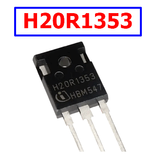
igbt H20R1353 datasheet pdf

Description

H20R1353 is a high-voltage insulated-gate bipolar transistor (IGBT) from the TRENCHSTOP family, designed specifically for resonant and soft-switching power electronics. Its 1350 V collector-emitter rating, high current capability, and integrated monolithic body diode make it particularly suitable for half-bridge and full-bridge power stages where the switching device must tolerate substantial voltage stress while operating with controlled commutation.
From a circuit-design perspective, the IHW20N135R3 combines a high voltage blocking capability with relatively low conduction loss and a diode intended for soft commutation. The positive temperature coefficient of its collector-emitter saturation voltage also makes current sharing between parallel devices more manageable than with devices exhibiting strongly negative thermal behavior.Typical applications include induction cookers, inverterized microwave ovens, resonant power supplies, induction heating equipment, soft-switching DC-DC converters, and other high-frequency power conversion systems.

Features

  • 1350 V collector-emitter rating: The high blocking-voltage capability is one of the main reasons to consider this IGBT in high-voltage resonant converters.
  • 20 A continuous current capability at elevated case temperature
  • 60 A pulsed collector current
  • Integrated body diode: The monolithic diode provides an internal current path during reverse conduction intervals. It is intended for soft commutation, so the circuit should not be designed around unnecessarily aggressive hard reverse-recovery operation.
  • Low VCE(sat): A relatively low saturation voltage helps reduce conduction loss when the IGBT is carrying substantial current. This is particularly useful in resonant converters where the device may conduct high peak currents even though the average power may be lower.
  • Positive temperature coefficient: The positive temperature behavior of VCE(sat) helps distribute current between paralleled IGBTs because a hotter device tends to develop a higher conduction voltage and therefore becomes less attractive for additional current.
  • ±20 V gate-emitter operating range
  • High pulsed current capability
  • Turn-off SOA: The switching stage must remain within the device’s turn-off safe operating area. Voltage, current, temperature, gate resistance, and commutation speed all influence whether the switching event is safe.

Pinout
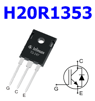
igbt H20R1353 pinout

Absolute Maximum Ratings (Tc = 25 °C)

Parameter Symbol Rating Unit
Collector-emitter voltage VCE 1350 V
DC collector current at Tc = 25 °C IC 40.0 A
DC collector current at Tc = 100 °C IC 20.0 A
Pulsed collector current ICpuls 60.0 A
Non-repetitive peak collector current ICSM 200 A
Diode forward current at Tc = 25 °C IF 40.0 A
Diode forward current at Tc = 100 °C IF 20.0 A
Pulsed diode current IFpuls 60.0 A
Gate-emitter voltage VGE ±20 V
Transient gate-emitter voltage, tp ≤ 10 μs, D < 0.010 VGE ±25 V
Power dissipation at Tc = 25 °C Ptot 310.0 W
Power dissipation at Tc = 100 °C Ptot 155.0 W
Operating junction temperature Tvj −40 to +175 °C
Storage temperature Tstg −55 to +175 °C

Typical Circuit Configurations

  • Half-bridge resonant converter: Two IGBTs can form a half-bridge driving an LC resonant network. This arrangement is common in induction heating and other high-frequency power conversion systems.
  • Full-bridge resonant inverter: Four devices can be arranged as a full bridge to apply alternating polarity to a resonant load or transformer primary. The integrated diodes provide current paths during commutation intervals.
  • Series-resonant converter: The IGBT bridge excites a series combination of inductive and capacitive elements. When correctly tuned, the resonant current and voltage waveforms can reduce switching stress.
  • LLC-type resonant stage: An LLC converter can use the IGBT in the primary switching bridge when the operating voltage, switching frequency, and loss profile are compatible with the device.
  • Induction heating inverter: A resonant tank consisting of an induction coil and capacitive network can be driven by a bridge or half-bridge. Soft switching is particularly important because current and voltage can be substantial.

Performance Advantages

  • Large voltage headroom: The 1350 V blocking rating is attractive in systems where DC-link transients make lower-voltage IGBTs uncomfortable from a reliability perspective.
  • Good fit for soft switching: Resonant switching can reduce turn-on and turn-off stress, allowing the device to operate efficiently at frequencies where conventional hard-switched approaches become increasingly lossy.
  • Integrated diode: A monolithic diode eliminates the need for a separately packaged freewheeling diode in many bridge configurations and can simplify the power-stage layout.
  • Low EMI potential: When the switching transition is properly controlled and the commutation is soft, the resulting waveform can reduce the high-frequency energy that commonly creates electromagnetic compatibility problems.

Typical Applications

  • Induction cooktops: Resonant inverter stages require switches capable of handling high voltage and substantial circulating current while maintaining controlled switching losses.
  • Induction heating equipment
  • Inverterized microwave ovens
  • Resonant DC-DC converters
  • Soft-switching power supplies
  • Industrial power electronics

IGBT H20R1353 Datasheet PDF

H20R1353 igbt

H20R1353 pdf

7342EK Datasheet PDF – 30V, 67A, MOSFET ( SM7342EKKP )

7342EK MOSFET is suitable for use as a desktop computer power management and DC/DC converter.

Part Number: SM7342EKKP

Function: 30V, Dual N-Channel MOSFET

Package: DFN5X6 Type

Manufacturer: Sinopower Semiconductor ( www.sinopowersemi.com )

Images

7342EK datasheet pdf

Description

7342EK is a dual N-channel enhancement-mode MOSFET in a DFN5x6G-8_EP2 package, integrating two power MOSFET dies with a 30V drain-source rating and optimized low-resistance switching characteristics. Channel 1 provides up to 67A continuous drain current with RDS(ON) of 4.3mΩ at VGS=10V, while Channel 2 provides up to 100A with RDS(ON) of 2mΩ at VGS=10V and includes an integrated Schottky diode. Typical applications include desktop computer power management, DC/DC converters, high-current load switching, and compact power conversion systems where low conduction loss and reduced PCB area are important.

Features

  • Channel 1 supports up to 67A continuous drain current at TC=25°C
  • Channel 2 supports up to 100A continuous drain current at TC=25°C
  • Channel 1 includes ESD protection
  • Channel 2 includes an integrated Schottky diode
  • 100% UIS and Rg tested
  • Low Qg and Qgd for high-speed switching
  • Low RDS(ON) for reduced conduction losses
  • Dual-die construction minimizes PCB space requirements
  • Maximum junction temperature of 150°C
  • Reliable and rugged construction for power switching applications

Pinout

pinout 7342EK mosfet SM7342EKKP

Absolute Maximum Ratings (Tc = 25 °C)

Parameter Symbol Value Unit
Drain-Source Voltage VDSS 30 V
Gate-Source Voltage, Channel 1 VGSS ±20 V
Gate-Source Voltage, Channel 2 VGSS ±12 V
Continuous Drain Current, Channel 1 at TC=25°C ID 67 A
Continuous Drain Current, Channel 2 at TC=25°C ID 100 A
Continuous Drain Current, Channel 1 at TC=100°C ID 42 A
Continuous Drain Current, Channel 2 at TC=100°C ID 86 A
Pulse Drain Current, Channel 1 IDM 268 A
Pulse Drain Current, Channel 2 IDM 400 A
Diode Continuous Forward Current, Channel 1 IS 14 A
Diode Continuous Forward Current, Channel 2 IS 28 A
Maximum Power Dissipation, Channel 1 at TC=25°C PD 31.25 W
Maximum Power Dissipation, Channel 2 at TC=25°C PD 62.5 W
Maximum Power Dissipation, Channel 1 at TC=100°C PD 12.5 W
Maximum Power Dissipation, Channel 2 at TC=100°C PD 25 W
Maximum Junction Temperature TJ 150 °C
Storage Temperature Range TSTG -55 to 150 °C
Thermal Resistance, Junction to Case, Channel 1 RθJC 4 °C/W
Thermal Resistance, Junction to Case, Channel 2 RθJC 2 °C/W
Continuous Drain Current, Channel 1 at TA=25°C ID 14 A
Continuous Drain Current, Channel 2 at TA=25°C ID 22 A
Continuous Drain Current, Channel 1 at TA=70°C ID 11 A
Continuous Drain Current, Channel 2 at TA=70°C ID 18 A
Pulse Drain Current, Channel 1 at TA=25°C IDM 56 A
Pulse Drain Current, Channel 2 at TA=25°C IDM 88 A
Maximum Power Dissipation, Channel 1 at TA=25°C PD 1.39 W
Maximum Power Dissipation, Channel 2 at TA=25°C PD 1.67 W
Thermal Resistance, Junction to Ambient, Steady State, Channel 1 RθJA 90 °C/W
Thermal Resistance, Junction to Ambient, Steady State, Channel 2 RθJA 75 °C/W
Avalanche Current, Single Pulse, L=0.1mH, Channel 1 IAS 24 A
Avalanche Current, Single Pulse, L=0.1mH, Channel 2 IAS 45 A
Avalanche Energy, Single Pulse, L=0.1mH, Channel 1 EAS 28.8 mJ
Avalanche Energy, Single Pulse, L=0.1mH, Channel 2 EAS 101.25 mJ

Working Principle

  • SM7342EKKP integrates two independent N-channel enhancement-mode MOSFET dies into a single compact package to reduce PCB area and simplify high-current power-stage layouts
  • Applying a positive gate-source voltage creates a conductive channel and reduces the drain-source resistance, allowing high current to flow with low conduction loss
  • Channel 1 is optimized for high-current switching and incorporates ESD protection for improved robustness during handling and circuit operation
  • Channel 2 combines a very low RDS(ON) MOSFET with an integrated Schottky diode, providing a low-loss current path for switching converter applications
  • The extremely low RDS(ON) values reduce conduction losses according to the I²R relationship, which is particularly important in high-current DC/DC converters
  • Low Qg and Qgd reduce the charge required to switch the MOSFET gates and help improve switching speed and overall converter efficiency
  • The integrated Schottky diode in Channel 2 can provide a low-forward-voltage freewheeling path during appropriate switching intervals
  • The 100% UIS testing and avalanche specifications provide additional robustness against controlled inductive switching transients

Design Notes

  • Keep the drain-source voltage below the 30V VDSS rating, including switching overshoot and transient conditions
  • Observe the different gate-source voltage limits of the two channels, with Channel 1 rated at ±20V and Channel 2 rated at ±12V
  • Use an appropriate gate-driver voltage to achieve the specified low RDS(ON) values while avoiding excessive gate voltage
  • Keep gate-drive loops short and minimize parasitic inductance to reduce ringing and unwanted gate-voltage overshoot
  • Use low-impedance PCB copper paths for the high-current drain and source connections to minimize additional conduction loss
  • Take advantage of the Kelvin-like or exposed-pad package layout where appropriate to improve thermal and electrical performance
  • Account for both MOSFET conduction loss and switching loss when calculating junction temperature

Applications

  • Desktop computer power management
  • DC/DC converters
  • High-current switching regulators
  • Power management systems
  • Load switching
  • Battery power conversion
  • High-frequency switching power supplies
  • Compact synchronous power stages
  • Low-loss power conversion circuits

Frequently Asked Questions

  • What is the maximum drain-source voltage? The common VDSS rating is 30V for both channels
  • What is the RDS(ON) of Channel 1? Channel 1 has a maximum RDS(ON) of 4.3mΩ at VGS=10V and 7.2mΩ at VGS=4.5V
  • What is the RDS(ON) of Channel 2? Channel 2 has a maximum RDS(ON) of 2mΩ at VGS=10V and 2.5mΩ at VGS=4.5V
  • What is the continuous drain current? At TC=25°C, Channel 1 is rated for 67A and Channel 2 is rated for 100A under the specified conditions
  • Does 7342EK include a diode? Yes, Channel 2 includes an integrated Schottky diode for appropriate power-switching and freewheeling applications

7342EK Datasheet PDF Download ( SM7342EKKP )

SM7342EKKP pdf

7342EK pdf