TL084 Datasheet – JFET-Input Operational Amplifier – TI

Part Number: TL084

Function : JFET-Input Operational Amplifier

Manufacturer: Texas Instruments

Image
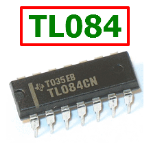
tl084-operational-amplifier

Description

The TL084 JFET-input operational amplifier family is designed to offer a wider selection than any previously developed operational amplifier family. Each of these JFET-input operational amplifiers incorporates well-matched, high-voltage JFET and bipolar transistors in a monolithic integrated circuit.

The devices feature high slew rates, low input bias and offset currents, and low offset-voltage temperature coefficient.

Pinout
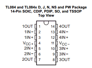
TL084 datasheet pinout

Features

1. Low Power Consumption: 1.4 mA/ch Typical
2. Wide Common-Mode and Differential Voltage Ranges
3. Low Input Bias Current: 30 pA Typical
4. Low Input Offset Current: 5 pA Typical
5. Output Short-Circuit Protection
6. Low Total Harmonic Distortion: 0.003% Typical
7. High Input Impedance: JFET Input Stage
8. Latch-Up-Free Operation
9. High Slew Rate: 13 V/μs Typical
10. Common-Mode Input Voltage Range Includes Vcc+

TL084 Schematic


Official Hompage : https://www.ti.com/product/tl084


TL084 Datasheet

PDF Download : https://www.ti.com/lit/ds/symlink/tl084.pdf


Related articles across the web

TLV62080 Datasheet PDF – 1.2A, Step Down Converter

Part Number: TLV62080

Package: WSON 8 Type

Function: 1.2A, High Efficient Step Down Converter

Power Management > DC/DC Switching Regulator > Converter (Integrated Switch) > Step-Down (Buck) Converter > TI TLV62080

The TLV62080 and TLV62084 devices are low cost buck converters in small size with less external components. They are synchronous step-down converters with an input voltage range of 2.5 and 2.7 (2.5 V for TLV62080, 2.7 V for TLV62084) to 5.5 V. The TLV6208x device focuses on high-efficiency step-down conversion over a wide output current range. At medium to heavy loads, the TLV6208x converter operates in PWM mode and automatically enters power save mode operation at light-load currents to maintain high efficiency over the entire load current range.

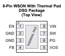
tlv62084tlv62084-pinout

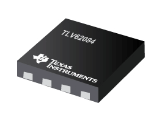
To address the requirements of system power rails, the internal compensation circuit allows a large selection of external output capacitor values ranging from 10-µF up to 100-uF effective capacitance. With the DCS-Control™ (Direct Control with Seamless transition into power save mode) architecture excellent load transient performance and output voltage regulation accuracy are achieved. The device is available in 2-mm × 2-mm WSON package with Thermal Pad.

2A High Efficient Step Down Converter

  • DCS-Control Architecture for Fast Transient Regulation
  • 2.5 to 5.5-V Input Voltage Range (TLV62080)
  • 2.7 to 5.5-V Input Voltage Range (TLV62084)
  • 100% Duty Cycle for Lowest Dropout
  • Power Save Mode for Light Load Efficiency
  • Output Discharge Function
  • Power Good Output
  • Thermal Shutdown
  • Available in 2 mm × 2 mm 8-Terminal WSON Package
  • For Improved Features Set, See the TPS62080 datasheet (SLVSAE8)

tlv62084-application

Official Site : https://www.ti.com/product/tlv62080

Other data sheets are available within the file:

TLV62080DSGR, TLV62080DSGT, TLV62084, TLV62084DSGR, TLV62084DSGT