AZC002-02N Datasheet – ESD Protection Diode Array ( PDF )

Part Number: AZC002-02N

Function: Low Capacitance ESD Protection Array For High Speed Data Interfaces

Package: SOT143-4L Type

Manufacturer: Amazing Microelectronic

Pinouts:
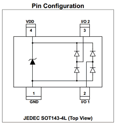
AZC002-02N datasheet


Description

The AZC002-02N is a high performance and low cost design which includes surge rated diode arrays to protect high speed data interfaces. The device family has been specifically designed to protect sensitive components, which are connected to data and transmission lines, from over-voltage caused by Electrostatic Discharging (ESD), Electrical Fast Transients (EFT), and Lightning.

Features

1. ESD Protect for 2 high-speed I/O channels
2. 5V operating voltage
3. Low capacitance : 1.2pF typical
4. Fast turn-on and Low clamping voltage
5. Array of surge rated diodes with internal equivalent TVS diode

Applications:

1. USB2.0 Power and Data lines protection
2. Notebook and PC Computers
3. Monitors and Flat Panel Displays
4. IEEE 1394 Firewire Ports

Other data sheets are available within the file: AZC002-02N.R7G

AZC002-02N Datasheet PDF Download


AZC002-02N pdf

OR2C26A Datasheet PDF – Field-Programmable Gate Array

Part Number: OR2C26A

Function: ORCA Feild-Programmable Gate Array. Voltage 5.0 V.

Package: 208, 240 SQFP, 304, 432 EBGA Pin Type

Manufacturer: Agere ( LSI Corporation )

Images:

OR2C26A datasheet


Description

The OR2C26A is Feild-Programmable Gate Arrays.

The ORCA Series 2 series of SRAM-based FPGAs are an enhanced version of the ATT2C/2T architecture. The latest ORCA series includes patented architectural enhancements that make functions faster and easier to design while conserving the use of PLCs and routing resources. The Series 2 devices can be used as drop-in replace ments for the ATT2Cxx/ATT2Txx series, respectively, and they are also bit stream compatible with each other.

The PLC architecture provides a balanced mix of logic and routing that allows a higher utilized gate/PFU than alternative architectures. The routing resources carry logic signals between PFUs and I/O pads. The routing in the PLC is symmetrical about the horizontal and vertical axes. This improves routability by allowing a bus of signals to be routed into the PLC from any direction.

What is FPGA?

FPGAs consist of a grid of configurable logic blocks (CLBs), which can be programmed to perform a variety of digital logic functions. These logic blocks can be interconnected using programmable routing resources, which allow designers to create custom digital circuits with high levels of flexibility and functionality.

FPGAs are programmed using hardware description languages (HDLs), such as Verilog or VHDL, which allow designers to specify the behavior of the digital circuit in a high-level language. The HDL code is then compiled into a configuration file, which is loaded onto the FPGA to configure the logic blocks and interconnects.

Features

1. Eight 3-state buffers per PFU for on-chip bus structures
2. High-performance, cost-effective, low-power 0.35 μm CMOS technology (OR2CxxA),
3. Full PCI bus compliance for all devices


Other data sheets are available within the file:

OR2C04A, OR2C06A, OR2C08A, OR2C10A, OR2C12A,
OR2C15A, OR2C40A, OR2C12A-4S240

OR2C26A Datasheet PDF Download


OR2C26A pdf