Part Number: JM20330
Function : Serial ATA Bridge Chip
Package: 64-pin TQFP Type
Manufacturer: JMicron ( http://www.jmicron.com/ )
Image
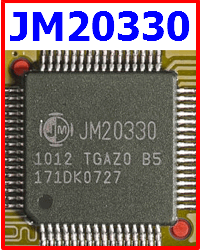
Description
JMicron’s JM20330 is a single chip solution for serial and parallel ATA translation. It includes the Serial ATA PHY, Link, Transport, and Parallel ATA (application layer) controller.
The Serial ATA physical, link, and transport layers are compliant to Serial ATA 1.0. JM20330 supports a 1.5GHz data rate, and scalable to 3.0 GHz data rate by directly doubling the internal clock source. The application layer supports both the ATA register command set and PACKET command set, which could drive both Hard Disk Drive and ATAPI Optical Storage such as CR-ROM, CD-RW, DVD-ROM, DVD-RW, etc.
The Serial ATA and the Parallel ATA application layer support both host and device operation and can be configured through a single pin.
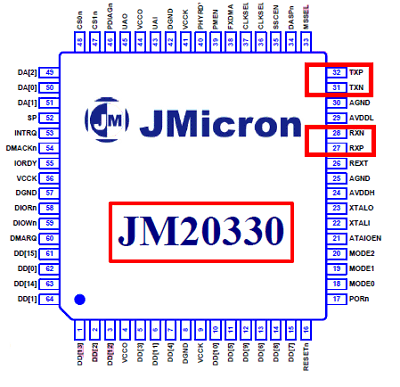
Pinout
Features
1. Serial ATA 1.0 Specification compliant
2. Automatic Serial ATA 3.0/1.5 Gbps speed negotiation
3. ATA/ATAPI PIO mode 0 to 4
4. ATA/ATAPI Ultra DMA of transfer rate 16.7, 25, 33, 48, 66, 100, 133, and 150MB/s.
5. ATA/ATAPI LBA48 addressing mode associated with 2-byte sector count
6. Support Serial ATA hot-plug
7. Ultra low power consumption
8. Work for both AC and DC couple between the transmitter and the receiver
9. Provide specified OOB signal detection and transmission
Reference Site: https://msfn.org/board/topic/152483-sata-to-ide-adapters-whichwhatwhy/
JM20330 Datasheet PDF