ADM7170 Datasheet PDF – 6.5 V, 500 mA, CMOS LDO

Part Number: ADM7170

Function: 6.5 V, 500 mA, Ultralow Noise, High PSRR, Fast Transient Response CMOS LDO

Package: 8-lead, 3 mm × 3 mm LFCSP Type

Manufacturer: Analog Devices

Image

ADM7170 LDO Voltage Regulator

Description

The ADM7170 is a CMOS, low dropout linear regulator (LDO) that operates from 2.3 V to 6.5 V and provides up to 500 mA of output current. This high output current LDO is ideal for regulation of high performance analog and mixed signal circuits operating from 6 V down to 1.2 V rails. Using an advanced proprietary architecture, the device provides high power supply rejection and low noise, and achieves excellent line and load transient response with just a small 4.7 µF ceramic output capacitor. Load transient response is typically 1.5 μs for a 1 mA to 500 mA load step.

Pinouts:
ADM7170 datasheet

Features

1. Input voltage range: 2.3 V to 6.5 V
2. Maximum load current: 500 mA
3. Low noise: 5 μV rms independent of output voltage at 100 Hz to 100 kHz
4. Fast transient response: 1.5 μs for 1 mA to 500 mA load step
5. 60 dB PSRR at 100 kHz

Application Circuit

components

Applications:

1. Communications and infrastructure

2. Medical and healthcare

3. Industrial and instrumentation

ADM7170 Datasheet PDF Download

ADM7170 pdf


Other data sheets are available within the file:

ADM7170ACPZ, ADM7170ACPZ-1.3-R7, ADM7170ACPZ-1.8-R7, ADM7170ACPZ-2.5-R7
74HC123 Datasheet PDF – CD74HC123PWT PDF – TI

Part Number: 74HC123, CD74HC123PWT

Function: High-Speed CMOS Logic Dual Retriggerable Monostable Multivibrators with Resets

Package: DIP, SOIC 16 Pin Type

Manufacturer: Texas Instruments

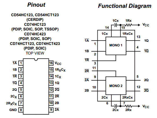
Pinout

74HC123 Pinout ti

Description

The 74HC123, 74HCT123, CD74HC423 and CD74HCT423 are dual monostable multivibrators with resets. They are all retriggerable and differ only in that the 123 types can be triggered by a negative to positive reset pulse; whereas the 423 types do not have this feature. An external resistor (RX) and an external capacitor (CX) control the timing and the accuracy for the circuit. Adjustment of Rx and CXprovides a wide range of output pulse widths from the Q andQ terminals. Pulse triggering on the A and B inputs occur at a
particular voltage level and is not related to the rise and fall times of the trigger pulses.

Once triggered, the output pulse width may be extended by retriggering inputs A and B. The output pulse can be terminated by a LOW level on the Reset (R) pin. Trailing edge triggering (A) and leading edge triggering (B) inputs are provided for triggering from either edge of the input pulse. If either Mono is not used each input on the unused device (A, B, andR) must be terminated high or low. The minimum value of external resistance, Rx is typically 5kΩ. The minimum value external capacitance, CX, is 0pF. The calculation for the pulse width is tW= 0.45 RXCX at VCC= 5V.

74HC123 Datasheet

Features

• Overriding Reset Terminates Output Pulse

• Triggering From the Leading or Trailing Edge

• Q and Q Buffered Outputs

• Separate Resets

• Wide Range of Output-Pulse Widths

• Schmitt Trigger on Both A and B Inputs

74HC123 Datasheet


Related articles across the web