ADS8354 Datasheet PDF – 16-Bit, Analog-to-Digital Converter

Part Number: ADS8354

Function: Dual, High-Speed, 16-Bit, Simultaneous-Sampling, Analog-to-Digital Converter

Package: WQFN-16 (3-mm ×3-mm) and TSSOP-16 Type

Manufacturer: Texas Instruments

Pinouts:
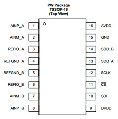
ADS8354 datasheet


Description

The ADS8354, ADS7854, and ADS7254 belong to a family of pin-compatible, dual, high-speed, simultaneous-sampling, analog-to-digital converters(ADCs) that support fully-differential analog inputs.

Each device includes two individually programmable reference sources that can be used for system-level gain calibration. Also, a flexible serial interface that can operate over a wide power-supply range enables easy communication with a large variety of host controllers.

Power consumption for a given throughput can be optimized by using the two low-power modes supported by the device. All devices are fully specified over the extended industrial temperature range (–40°C to 125°C) and are available in pin-compatible, WQFN-16 (3-mm ×3-mm) and TSSOP-16 packages.

Application Circuits :

components

Features

1. Simultaneous Sampling of Two Channels

2. Supports Fully-Differential Inputs

3. Dual, Programmable, and Buffered 2.5-V Internal Reference

Applications:

1. Protection Relays

2. Power Quality Measurement

3. Three-Phase Power Controls


Other data sheets are available within the file:

7254, 7854, 8354, ADS7254, ADS7254IPW


ADS8354 Datasheet PDF Download


ADS8354 pdf

AD7951 Datasheet PDF – Programmable Input PulSAR ADC

Part Number: AD7951

Function: 14-Bit, 1 MSPS, Unipolar/Bipolar Programmable Input PulSAR ADC

Package: 48-lead LQFP and LFCSP (7 mm × 7 mm) Type

Manufacturer: Analog Devices

Pinouts:

AD7951 datasheet


Description

The AD7951 is a 14-bit, charge redistribution, successive approximation register (SAR) architecture analog-to-digital converter (ADC) fabricated on Analog Devices, Inc.’s iCMOS high voltage process. The device is configured through hardware or via a dedicated write only serial configuration port for input range and operating mode. The AD7951 contains a high speed 14-bit sampling ADC, an internal conversion clock, an internal reference (and buffer), error correction circuits, and both serial and parallel system interface ports.

A falling edge on CNVST samples the analog input on IN+ with respect to a ground sense, IN−. The AD7951 features four different analog input ranges and three different sampling modes: warp mode for the fastest throughput, normal mode for the fastest asynchronous throughput, and impulse mode where power is scaled with throughput. Operation is specified from −40°C to +85°C.

Features

1. Multiple pins/software programmable input ranges : 2.5 V, 10 V, ±5 V, ±10 V
2. Pins or serial SPI® compatible input ranges/mode selection
3. 14-bit resolution with no missing codes
4. INL: ±0.3 LSB typ, ±1 LSB max (±61 ppm of FSR) SNR: 85 dB @ 2 kHz
5. iCMOS® process technology
6. 5 V internal reference: typical drift 3 ppm/°C; TEMP output
7. No pipeline delay (SAR architecture)
8. Parallel (14- or 8-bit bus) and serial 5 V/3.3 V interface

Applications

1. Process control
2. Medical instruments
3. High speed data acquisition
4. Digital signal processing
5. Instrumentation
6. Spectrum analysis
7. ATE

Other data sheets are available within the file:

AD7951BCPZ, AD7951BCPZRL, AD7951BSTZ, AD7951BSTZRL


AD7951 Datasheet PDF Download


AD7951 pdf