VDS7616A4A-6 Datasheet PDF – 166Mhz, Synchronous DRAM

Part Number: VDS7616A4A-6

Function: 2 M x 16 Bit x 4 Banks, Synchronous DRAM

Package: 400mil 54pin TSOPII

Manufacturer: A-Data Technology

Image and Pinouts:
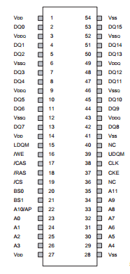
VDS7616A4A-6 datasheet

Description

The VDS7616A4A-6 are four-bank Synchronous DRAMs organized as 2,097152 words x 16 bits x 4 banks. Synchronous design allows precise cycle control with the use of system clock I/O transactions are possible on every clock cycle. Range of operating frequencies, programmable burst length and programmable latencies allow the same device to be useful for a variety of high bandwidth high performance memory system applications.

Features

1. JEDEC standard LVTTL 3.3V power supply

2. MRS Cycle with address key programs
(1) CAS Latency (2 & 3)
(2) Burst Length (1,2,4,8,& full page)
(3) Burst Type (sequential & Interleave)

3. 4 banks operation

4. All inputs are sampled at the positive edge of the system clock

5. Burst Read single write operation

6. Auto & Self refresh

7. 4096 refresh cycle

8. DQM for masking


Other data sheets are available within the file: VDS7616A4A-55, VDS7616A4A, VDS7616A4A-7

VDS7616A4A-6 Datasheet PDF Download


VDS7616A4A-6 pdf


M28W320 Datasheet – 32 Mbit, Flash Memory ( PDF )

Part Number: M28W320

Function: 32 MBIT (2MB X16, BOOT BLOCK) LOW VOLTAGE FLASH MEMORY

Package: TFBGA47, TSOP48 Type

Manufacturer: STMicroelectronics

Pinouts:

M28W320 datasheet


Description

The M28W320 is a 32 Mbit (2 Mbit x 16) nonvolatile Flash memory that can be erased electricallyat the block level and programmed in-system on aWord-by-Word basis. These operations can beperformed using a single low voltage (2.7 to 3.6V)supply. VDDQallows to drive the I/O pin down to1.65V. An optional 12V VPPpower supply is pro-vided to speed up customer programming.

Features

1. Supply Voltage

(1) Vdd = 2.7V to 3.6V Core Power Supply
(2) Vddq = 1.65V to 3.6V for Input/Output
(3) Vpp= 12V for fast Program (optional)

2. Access Time: 70, 80, 90, 100ns

3. Programming Time

(1) 10µs typical
(2) Double Word Programming Option
(3) Quadruple Word Programming Option

4. Common Flash Interface

5. Memory Blocks

(1) Parameter Blocks (Top or Bottom location)
(2) Main Blocks

6. Block Locking

(1) All blocks locked at Power Up
(2) Any combination of blocks can be locked
(3) WP for Block Lock-Down

Other data sheets are available within the file:

M28-W320, M28W320FCB, M28W320FCT


M28W320 Datasheet PDF Download


M28W320 pdf