PSD935G2 Datasheet PDF – Configurable Memory System

Part Number: PSD935G2

Function: Configurable Memory System on a Chip for 8-Bit Microcontroller

Package: TQFP-80 Type

Manufacturer: STMicroelectronics

Image and Pinouts:
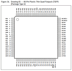
PSD935G2 datasheet

Description

The PSD935G2 series of Programmable Microcontroller (MCU) Peripherals brings In-System-Programmability (ISP) to Flash memory and programmable logic. The result is a simple and flexible solution for embedded designs. PSD9XX devices combine many of the peripheral functions found in MCU based applications :

1. 4 Mbit of Flash memory

2. A secondary Flash memory for boot or data

3. Over 3,000 gates of Flash programmable logic

4. 64 Kbit SRAM

5. Reconfigurable I/O ports

6. Programmable power management.

Features

1. 5V ± 10% Single Supply Voltage

2. Up to 4 Mbit of Primary Flash Memory (8 uniform sectors)

3. 256Kbit Secondary Flash Memory (4 uniform sectors)

4. Up to 64 Kbit SRAM

5. Over 3,000 Gates of PLD: DPLD

6. 52 Reconfigurable I/O ports

7. Enhanced JTAG Serial Port

8. Programmable power management

Other data sheets are available within the file: PSD935G, PSD935G2V, PSD935G3V-70J, PSD913G2, PSD934F2

PSD935G2 Datasheet PDF Download

PSD935G2 pdf

25L8006E Datasheet – Serial Flash Memory – MXIC

Part Number: 25L8006E, MX25L8006E

Function: 8M-BIT [x 1 / x 2] CMOS SERIAL FLASH

Package: 8-pin SOP,  8-pin PDIP (300mil), 8-land WSON (6x5mm)

Manufacturer: MXIC

Images:
25L8006E Flash Memory

Description

The 25L8006E feature a serial peripheral interface and software protocol allowing operation on a simple 3-wire bus. The three bus signals are a clock input (SCLK), a serial data input (SI), and a serial data output (SO). Serial access to the device is enabled by CS# input.  When it is in Dual Output read mode, the SI and SO pins become SIO0 and SIO1 pins for data output. The device provides sequential read operation on whole chip.
After program/erase command is issued, auto program/erase algorithms which program/erase and verify the specified page or sector/block locations will be executed. Program command is executed on byte basis, or page basis, or word basis for erase command is executes on sector, or block, or whole chip basis.

Pinout
25L8006E pinout datasheet

General

Features

• Single Power Supply Operation
– 2.7 to 3.6 volt for read, erase, and program operations

• Serial Peripheral Interface compatible — Mode 0 and Mode 3

• 8,388,608 x 1 bit structure or 4,194,304 x 2 bits (Dual Output mode) structure

• 256 Equal Sectors with 4K byte each
– Any Sector can be erased individually

• 16 Equal Blocks with 64K byte each
– Any Block can be erased individually

• Program Capability
– Byte base
– Page base (256 bytes)

• Latch-up protected to 100mA from -1V to Vcc +1V

PERFORMANCE

• High Performance
– Fast access time: 86MHz serial clock
– Serial clock of Dual Output mode : 80MHz
– Fast program time: 1.4ms(typ.) and 5ms(max.)/page
– Byte program time: 9us (typical)
– Fast erase time: 60ms(typ.) /sector ; 0.7s(typ.) /block

• Low Power Consumption
– Low active read current: 12mA(max.) at 86MHz
– Low active programming current: 20mA (max.)
– Low active erase current: 20mA (max.)
– Low standby current: 25uA (max.)
– Deep power-down mode 5uA (typical)

• Typical 100,000 erase/program cycles

• 20 years of data retention

[…]

25L8006E Datasheet PDF

Related articles across the web