B4300CR-5.1 Datasheet PDF – 300mA, 5.1V, LDO Regulator

Part Number: B4300CR-5.1

Function: 300mA, 5.1V, CMOS Low Dropout Regulator

Package: SOT-89 & SOT-223

Manufacturer: Bay Linear

Image and Pinouts:
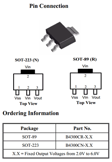
B4300CR-5.1 datasheet


Description

The B4300CR-5.1 series are a group of positive output voltage, three-pin regulators, which provide a high current even when the input/output voltage differential is small. Low power consumption and high accuracy is achieved though CMOS and programmable fuse technologies. Output voltage: 2.0V to 6.0V in 0.1V increments. The B4300 consists of a high-precision voltage reference, an error correction circuit, and a current limited output driver. Available in SOT-89 (300mW), and SOT-223 (500mW) packages minimizing the usage of board real state.

Features

1. Maximum output current: 300 mA.

2. Highly accurate: Output voltage +/- 1.4%

3. Extremely Low Ground Current 6μA

4. CMOS low power consumption.

5. Over-Current & Over-Temp. Protection

6. Pin-to-Pin replacement for TC1108 & XC6203


Absolute Maximum Ratings :

1. Input Voltage : VIN = 6.5 V

2. Output Current : IOUT = 300 mA

3. Output Voltage : VOUT = VSS -0.3 to VIN 0.3 V

4. Continual Total Power Dissipation
(1) SOT-89 : Pd = 300 mW
(2) SOT-223 : Pd = 500 mW

Applications:

1. Battery Powered Equipment

2. Notebook PC, Palmtops, PDA

3. Portable Cameras and Video Recorders

4. Reference Voltage Sources

Other data sheets are available within the file:

B4300CN-2.0, B4300CN-2.2, B4300CN-2.3, B4300CN-2.4, B4300CN-2.5

B4300CR-5.1 Datasheet PDF Download


B4300CR-5.1 pdf


APL5551 Datasheet PDF – Dual Channel Regulator

Part Number: APL5551

Function: Dual Channel 500mA/500mA Regulator + Reset IC

Package: SOP-8 Pin Type

Manufacturer: Anpec Electronics

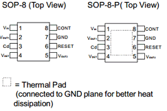
Image and Pinouts:

APL5551 datasheet


Description

The APL5551 is a dual-channel regulator with reset function (specific voltage monitoring), and internal delay circuit, set to detect 3.9V. Maximum input voltage is 6V, and both output1 and output2 can deliver up to 450mA. The typical dropout voltage of both channel is 500mV at 500mA loading. Design with an internal P-channel MOSFET pass transistor , the APL5551 maintains  a low  supply curr ent . Other feat ures include, thermal-shutdown protecti on,  current limit protection to ensure specified output current. The APL5551 comes in miniature SOP-8 and OP-8-P packages.

Features

1. Low Quiescent Current : 110µA  (No load)

2. Low Dropout Voltage  :
(1) VDROP1 = 450mV @ 500mA
(2) VDROP2 = 500mV @ 500mA

3. Fixed Output Voltage :
(1) VOUT1 = 3.3V/500mA
(2) VOUT2 = 2.8V/500mA

4. Stable  with 4.7mF  Output  Ca pacitor

5. Stable  with  Aluminum,  Tantalum  or  Ceramic Capacitors

6. Built  in  Thermal  Protection

7. Fast  Transient Response

8. Short  Setting  Time

9. SOP-8, SOP-8-P  with  Thermal Pad Packages

10. Adjustment-free  Reset  Detection  Voltage :3.9V  typ

11. Easy  to Set  Delay  Time from  Voltage Detection to Reset Release

12. Lead Free Available (RoHS Compliant)

Applications:

  1. Optical Storage System

Other data sheets are available within the file: APL5551K, APL5551KA

APL5551 Datasheet PDF Download


APL5551 pdf