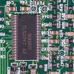
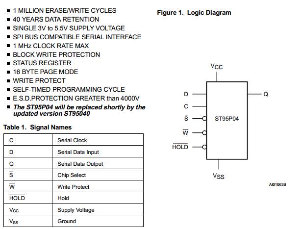
This is one of the semiconductor types.
This part name is 24C02WP.
This product has SERIAL 2K (256 x 8) EEPROM functions.
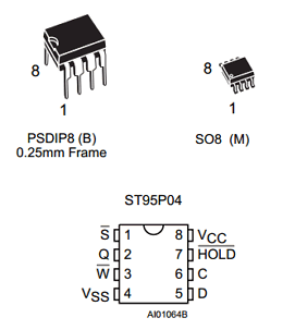
The package is SOP 8 pin type.
The manufacturer of the product is STMicroelectronics.
See the preview image and the PDF file for more information.
Image :

Description
This specification covers a range of 2K bits I2C bus EEPROM products, the ST24C02 / ST25C02, the ST24C02R and ST24W02 / ST25W02. In the text, products are referred to as ST24/25×02, where “x” is: “C” for Standard version and “W” for hardware Write Control version.
The ST24/25×02 are 2K bit electrically erasable programmable memories (EEPROM), organized as 256 x 8 bits. They are manufactured in SGS THOMSON’s Hi-Endurance Advanced CMOS technology which guarantees an endurance of one million erase/write cycles with a data retention of 40 years. The memories operate with a power supply value as low as 1.8V for the ST24C02R only.
Both Plastic Dual-in-Line and Plastic Small Outline packages are available.
Features
1. HARDWARE WRITE CONTROL VERSIONS : ST24W02 and ST25W02
2. TWO WIRE SERIAL INTERFACE, FULLY I2C BUS COMPATIBLE
3. BYTE and MULTIBYTE WRITE (up to 4 BYTES)
5. PAGE WRITE (up to 8 BYTES)
6. BYTE, RANDOM and SEQUENTIAL READ MODES
7. SELF TIMED PROGRAMMING CYCLE
24C02WP Datasheet PDF

Other data sheets are available within the file: 24C02WP, 24CO2WP, ST24C02, ST24C02R, ST24W02