INA128-HT Datasheet PDF – Instrumentation Amplifier – TI

Part Number: INA128-HT

Function : High Temperature Precision, Low Power Instrumentation Amplifier

Package: SOIC 8 Pin Type

Manufacturer: TI

Simplified Schematic
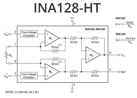
INA128-HT schematic

Description

The INA128-HT and INA129-HT are low-power, general-purpose instrumentation amplifiers offering excellent accuracy. The versatile three-operational-amplifier design and small size make them ideal for a wide range of applications. Current-feedback input circuitry provides wide bandwidth even at high gain. A single external resistor sets any gain from 1 to 10000. The INA128-HT provides an industry-standard gain equation; the INA129-HT gain equation is compatible with the AD620.

Features

1. Low Offset Voltage: 25 uV Typical

2. Low Input Bias Current: 50 nA Typical

3. High CMR: 95 dB Typical

4. Inputs Protected to ±40 V

5. Wide Supply Range: ±2.25 V to ±18 V

6. Low Quiescent Current: 2 mA Typical

Image and Pinout:

INA128-HT datasheet pinout


Applications:

1. Bridge Amplifiers

2. Thermocouple Amplifiers

3. RTD Sensor Amplifiers

4. Medical Instrumentation

5. Data Acquisition

Official Homepage: https://www.ti.com/product/INA128-HT

INA128-HT Datasheet PDF


ADS7042 Datasheet – 12-Bit, 1-MSPS, SAR ADC ( PDF )

Part Number: ADS7042

Function: Ultra-Low Power, Ultra-Small Size, 12-Bit, 1-MSPS, SAR ADC

Package: X2QFN, VSSOP 8 Pin

Manufacturer: Texas Instruments

Description

The ADS7042 is a 12-bit, 1-MSPS, analog-to-digital converter (ADC). The device supports a wide analog input voltage range (1.8 V to 3.6 V) and includes a capacitor-based, successive-approximation register (SAR) ADC with an inherent sample-and-hold circuit.

ADS7042 Pinouts

ADS7042 datasheet

The SPI-compatible serial interface is controlled by the CS and SCLK signals. The input signal is sampled with the CS falling edge and SCLK is used for conversion and serial data output. The device supports a wide digital supply range (1.65 V to 3.6 V), enabling direct interface to a variety of host controllers. The ADS7042 complies with the JESD8-7A standard for normal DVDD range (1.65 V to 1.95 V).

The IC is available in 8-pin, miniature, leaded, and X2QFN packages and is specified for operation rom –40°C to 125°C. Miniature form-factor and extremely low-power consumption make this device suitable for space-constrained, battery-powered applications.

The device is an ultralow-power, ultra-small analog-to-digital converter (ADC) that supports a wide analog input range. The analog input range for the device is defined by the AVDD supply voltage. The device samples the input voltage across the AINP and AINM pins on the CS falling edge and starts the conversion. The clock provided on the SCLK pin is used for conversion and data transfer. During conversions, both the AINP and AINM pins are disconnected from the sampling circuit. After the conversion completes, the sampling capacitors are reconnected across the AINP and AINM pins and the ADS7042 enters acquisition phase.

Applications:

• Low-Power Data Acquisition
• Battery-Powered Handheld Equipment
• Level Sensors
• Ultrasonic Flow Meters
• Motor Control
• Wearable Fitness

Other data sheets are available within the file:

7042, ADS7042IDCUR, ADS7042IDCUT, ADS7042IRUGR

ADS7042 Datasheet PDF Download


ADS7042 pdf

Related articles across the web