Part Number: SN74SSQEC32882
Function: 28-Bit to 56-Bit Registered Buffer With Address Parity Test One Pair to Four Pair Differential Clock PLL Driver
Package: NFBGA 176 Pin type
Manufacturer: Texas Instruments
Pinouts:
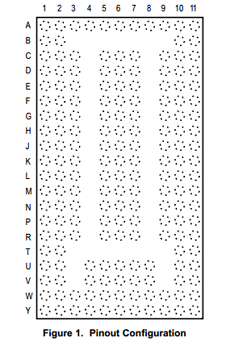
Description
The SN74SSQEC32882 implements different power saving mechanisms to reduce thermal power dissipation and to support system power down states. By disabling unused outputs the power consumption is further reduced.
The package is optimized to support high density DIMMs. By aligning input and output positions towards DIMM finger signal ordering and SDRAM ballout the device de-scrambles the DIMM traces allowing low cross talk design with low interconnect latency.
Edge controlled outputs reduce ringing and improve signal eye opening at the SDRAM inputs.
This 1:2 or 26-bit 1:2 and 4-bit 1:1 registering clock driver with parity is designed for operation on DDR3 registered DIMMs with VDD of 1.5 V, on DDR3L registered DIMMs with VDD of 1.35 V and on DDR3U registered DIMMs with VDD of 1.25 V.
Features
1. 1-to-2 Register Outputs and 1-to-4 Clock Pair Outputs Support Stacked DDR3 RDIMMs
2. CKE Powerdown Mode for Optimized System Power Consumption
3. 1.5V/1.35V/1.25V Phase Lock Loop Clock Driver for Buffering One Differential Clock Pair (CK and CK) and Distributing to Four Differential Outputs
4. 1.5V/1.35V/1.25V CMOS Inputs
5. Checks Parity on Command and Address (CS-Gated) Data Inputs
SN74SSQEC32882 Datasheet PDF Download


Other data sheets are available within the file:
EC32882S, 74SSQEC32882, SN74SSQEC32882ZALR
