CDCLVC1310 Datasheet PDF – Clock Fanout Buffer

Part Number: CDCLVC1310

Function: Ten-Output Low-Jitter Low-Power Clock Buffer and Level Translator

Package: 32P QFN Type.

Manufacturer: Texas Instruments

Pinouts:
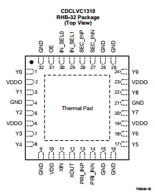
CDCLVC1310 datasheet


Description

The CDCLVC1310 is a highly versatile, low-jitter, low-power clock fanout buffer which can distribute to ten low-jitter LVCMOS clock outputs from one of three inputs, whose primary and secondary inputs can feature differential or single-ended signals and crystal input.


Features

1. High-Performance Crystal Buffer With Ultralow Noise Floor of –169 dBc/Hz

2. Additive Phase Noise/Jitter Performance Is 25 fsRMS (Typ.)

3.10 Single-Ended LVCMOS Outputs.


Applications:

1. Wireless and Wired Infrastructure

2. Networking and Data Communications

3. Portable Test and Measurement


Other data sheets are available within the file:

CDCLVC1310RHBR


CDCLVC1310 Datasheet PDF Download


CDCLVC1310 pdf

CD4011BC Datasheet PDF – Quad, NAND Buffered Gate

Part Number: CD4011BC

Function: Quad 2-Input NAND Buffered B Series Gate

Package: SOP 14, DIP 14  Pin Type

Manufacturer: Fairchild Semiconductor

Pinouts:

CD4011BC datasheet


Description

The CD4001BC and CD4011BC quad gates are monolithic complementary MOS (CMOS) integrated circuits constructed with N- and P-channel enhancement mode transistors.

They have equal source and sink current capabilities and conform to standard B series output drive. The devices also have buffered outputs which improve transfer characteristics by providing very high gain. All inputs are protected against static discharge with diodes to VDDand VSS.

Features

1. Low power TTL : Fan out of 2 driving 74L compatibility: or 1 driving 74LS

2. 5V–10V–15V parametric ratings

3. Symmetrical output characteristics

4. Maximum input leakage 1 µA at 15V over full temperature range

Other data sheets are available within the file:

CD4001BCM, CD4001BCN, CD4001BCSJ, CD4011


CD4011BC Datasheet PDF Download


CD4011BC pdf