8P34S1208 Datasheet PDF – Differential LVDS Fanout Buffer

Part Number: 8P34S1208

Function: 1:8 LVDS Output 1.8V Fanout Buffer

Package: VFQFN 28 Pin Type

Manufacturer: Integrated Device Technology

Image and Pinouts:
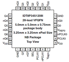
8P34S1208 datasheet


Description

The IDT 8P34S1208 is a high-performance differential LVDS fanout buffer. The device is designed for the fanout of high-frequency, very low additive phase-noise clock and data signals.

The 8P34S1208 is characterized to operate from a 1.8V power supply. Guaranteed output-to-output and part-to-part skew characteristics make the 8P34S1208i ideal for those clock distribution applications demanding well-defined performance and repeatability.

Two selectable differential inputs and eight low skew outputs are available. The integrated bias voltage reference enables easy interfacing of AC-coupled signals to the device inputs.

The device is optimized for low power consumption and low additive phase noise.

Features

1. Eight low skew, low additive jitter LVDS output pairs

2. Two selectable, differential clock input pairs

3. Differential CLK, nCLK pairs can accept the following differential input levels: LVDS, CML

4. Maximum input clock frequency: 1.5GHz

5. LVCMOS/LVTTL interface levels for the control input select pin

Other data sheets are available within the file: P34S1208, 8P34S1208i


8P34S1208 Datasheet PDF Download


8P34S1208 pdf

74VHCT244 Datasheet PDF – Octal Buffer / Line Driver

Part Number: 74VHCT244

Function: Octal Buffer/Line Driver with 3-STATE Outputs

Package: DIP, SOP, TSSOP 20 Pin Type

Manufacturer: Fairchild Semiconductor

Pinouts:

74VHCT244 datasheet


Description

The 74VHCT244, 74VHCT244A is an advanced high speed CMOS octal bus transceiver fabricated with silicon gate CMOS technology. It achieves high speed operation similar to equivalent Bipolar Schottky TTL while maintaining the CMOS low power dissipation. The VHCT244A is a non inverting 3-STATE buffer having two active-LOW output enables. This device is designed to be used as 3-STATE memory address drivers, clock drivers, and bus oriented transmitter/receivers.

Protection circuits ensure that 0V to 7V can be applied to the input and output (1) pins without regard to the supply voltage. These circuits prevent device destruction due to mismatched supply and input/output voltages. This device can be used to interface 5V to 3V systems and two supply systems such as battery back up.


Features

1. High Speed: tPD = 5.9 ns (typ) at VCC = 5V

2. Power down protection is provided on inputs and outputs

3. Low power dissipation: ICC = 4 µA (max) @ TA = 25°C

4. Pin and function compatible with 74HCT244


Other data sheets are available within the file:

74VHCT244ACW, 74VHCT244AM, 74VHCT244AMTC, 74VHCT244AMTCX

74VHCT244 Datasheet PDF Download


74VHCT244 pdf