AD404M42VT Datasheet PDF – 4M, CMOS Dynamic RAM

Part Number: AD404M42VT

Function: 4M, CMOS Dynamic RAM

Package: 26 Pin SOJ, 24 Pin TSOP Type

Manufacturer: ASCEND

Image and Pinouts:
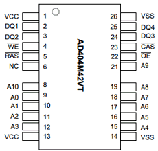
AD404M42VT datasheet


Description

The AD404M42VT is 4,194,304 words x 4 bits, CMOS Dynamic RAM.

The device CMOS Dynamic RAM organized as 4,194,304 words x 4 bits with extended data out access mode. It is fabricated with an advanced submicron CMOS technology and designed to operate from a Single 3.3V oniy power supply. Low voltage operation is more suitable to be used on battery backup, portable electronic application. lt is packaged in JEDEC standard 26/24-pin plastic SOJ or TSOP(II).

Features

1. Single 3.3V only power supply

2. High speed tRAC acess time : 50/60ns

3. Low power dissipation
(1)  Active mode : 432/396 mW (Mas)
(2)  Standby mode: 0.54 mW (Mas)

4. Extended – data – out(EDO) page mode access

5. I/O level: CMOS level (Vcc = 3.3V)

6. 2048 refresh cycle in 32 ms(Std.) or 128 ms(S-version)


Other data sheets are available within the file:

AD4016M326VQB-5, AD404M42VS, AD404M42VSA-5, AD404M42VSA-6, AD404M42VT


AD404M42VT Datasheet PDF Download

AD404M42VT pdf

Related articles across the web

25L1606E Datasheet – CMOS SERIAL FLASH MEMORY

Part Number: 25L1606E, MX25L1606E

Function: MXIC CMOS SERIAL FLASH MEMORY

Package: SOP8

Manufacturer: Macronix International

Image:
25L1606E

Description

This is 3V, 16M-Bit, CMOS Serial Flash Memory.

The device feature a serial peripheral interface and software protocol allowing operation on a simple 3-wire bus. The three bus signals are a clock input (SCLK), a serial data input (SI), and a serial data output (SO).

Serial access to the device is enabled by CS# input. When it is in Dual Output read mode, the SI and SO pins become SIO0 and SIO1 pins for data output. The device provides sequential read operation on whole chip. After program/erase command is issued, auto program/erase algorithms which program/erase and verify the specified page or sector/block locations will be executed. Program command is executed on byte basis, or page basis, or word basis for erase command is executes on sector, or block, or whole chip basis.

Pinouts:

25L1606E Datasheet

1. CS# : Chip Select
2. SI/SIO0 : Serial Data Input (for 1 x I/O)/ Serial Data Input & Output (for Dual Output mode)
3. SO/SIO1 : Serial Data Output (for 1 x I/O)/ Serial Data Output (for Dual Output mode)
4. SCLK : Clock Input
5. WP# : Write protection
6. HOLD# : Hold, to pause the device without deselecting the device
7. VCC : +3.3V Power Supply
8. GND : Ground

Features

1. Hold Feature
2. Low Power Consumption
3. Auto Erase and Auto Program Algorithms
4. Additional 512 bit secured OTP for unique identifier

Other data sheets are available within the file: 25L1606, MX25L1606E

25L1606E Datasheet PDF Download

25L1606E pdf


Related articles across the web