CD4514 Datasheet – CMOS 4-Bit Latch, 4-to-16 Line Decoder

Part Number: CD4514

Function  : CMOS 4-BIT LATCH/4-TO-16 LINE DECODERS

Package: DIP 24 Pin Type

Manufacturer: Texas Instruments

Image

CD4514 cmos decoder

Description

CD4514 and CD4515B consist of a 4-bit strobed latch and a 4-to-16-line decoder. The latches hold the last input data presented prior to the strobe transition from 1 to 0. Inhibit control allows all outputs to be placed at 0 (CD4514B) or 1 (CD4515B) regardless of the state of the data or strobe inputs.

The decode truth table indicates all combinations of data inputs and appropriate selected outputs.

These devices are similar to industry types MC14514 and MC14515.

CD4514 Circuit

CD4514 circuit


Features

1. Strobed input latch

2. Inhibit control

3. 100% tested for quiescent current at 20 V

4. Maximum input current of 1 µA at 18 V over full package-temperature range; 100 nA at 18 V and 25°C

Pinout

CD4514 datasheet pinout
Applications

1. Digital multiplexing

2. Address decoding

3. Hexadecimal/BCD decoding

4. Program-counter decoding

5. Control decoder

 
Official Homepage: https://www.ti.com/product/CD4514B

CD4514 Datasheet

#1. PDF Download : https://www.ti.com/lit/ds/symlink/cd4514b.pdf

#2. PDF Download : CD4514.PDF


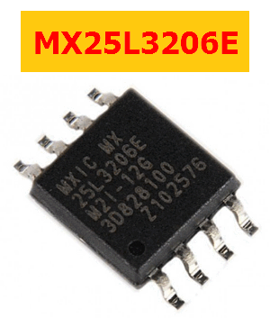
MX25L3206E Datasheet – 32M Bit CMOS Serial Flash – MXIC

Part Number: MX25L3206E

Function: 32M-BIT [x 1 / x 2] CMOS SERIAL FLASH

Manufacturer: Macronix International

Image :

MX25L3206E datasheet


Description

The MX25L3206E feature a serial peripheral interface and software protocol allowing operation on a simple 3-wire bus. The three bus signals are a clock input (SCLK), a serial data input (SI), and a serial data output (SO). Serial access to the device is enabled by CS# input. When it is in Dual Output read mode, the SI and SO pins become SIO0 and SIO1 pins for data output.


Pinout

MX25L3206E pinout
Features

1. Single Power Supply Operation
– 2.7 to 3.6 volt for read, erase, and program operations

2. Serial Peripheral Interface compatible — Mode 0 and Mode 3

3. 33,554,432 x 1 bit structure or 16,777,216 x 2 bits (Dual Output mode) structure

4. 1024 Equal Sectors with 4K byte each
– Any Sector can be erased individually

5. 64 Equal Blocks with 64K byte each
– Any Block can be erased individually

6. Program Capability
– Byte base
– Page base (256 bytes)

7. Latch-up protected to 100mA from -1V to Vcc +1V

MX25L3206E Datasheet PDF Download

25L3206E pdf


Other data sheets are available within the file: MX25L3206EMI-12G, MX25L3206EPI-12G, MX25L3206EZNI-12G

Related articles across the web