SDC7500 Datasheet – Voltage Mode PWM Controller – SDC

Part Number: SDC7500

Function: Voltage Mode PWM Controller

Package: DIP 16 Type

Manufacturer: Shaoxing Devechip Microelectronics ( http://www.sdc-semi.com )

Image :
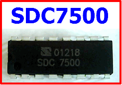
sdc7500-pwm-controller

Description

The SDC7500 is a voltage mode pulse width modulation switching regulator control circuit designed primarily for power supply control. The SDC7500 consists of a reference voltage circuit, two error amplifiers, an on-chip adjustable oscillator, a dead-time control (DTC) comparator, a pulse-steering control flip-flop, and an output control circuit. The precision of voltage reference (VREF) is ±1% through trimming and this provides a better output voltage regulation. The SDC7500 provides for push-pull or single-ended output operation, which can be selected through the output control.


Pinout
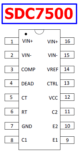
sdc7500-datasheet-pinout


Features

1. Complete PWM power control circuitry

2. Uncommitted outputs for 200mA sink or source current

3. Output control for single ended or push pull operation

4. Internal regulator provides a stable 5V reference supply with 5% tolerance

5. Adjustable dead-time control


Block Diagram
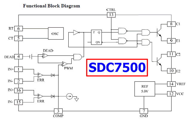
sdc7500-block-diagram

SDC7500 Datasheet

SDC7500 pdf


Related articles across the web

HT3582DA Datasheet PDF – Charger Controller Chip – Hotchip

Part Number: HT3582DA

Function: HT3582DA is a built-in reference voltage universal charger controller chip

Manufacturer: HOTCHIP TECHNOLOGY

Pinouts:
HT3582DA datasheet pinout

Description – HT3582DA

1. Maximum charge current: 300mA

2. Support for 0V battery charging (battery positive connection)

3. Automatic identification battery polarity

4. Short circuit protection

5. O
vertemperature protection

6. H
ighly integrated, very few external components

Battery load

When battery power communication and have not had access, the voltage difference between both ends of BTP and BTN 4.23V (typ), L1-L3 state
Description Table 3.

Normal charging and saturation detection

Power connectivity and access to full battery (battery voltage <4.10V [typical]), power began to pass control of the battery into HT3582DA
Line, the charging current of about 300mA (typ), gradually increasing the voltage across the battery when the battery voltage rises to 4.23V (typ)
When the battery is close to saturation, then transferred to a small current constant trickle charge mode. This process of state L1-L3 described in Table 3. when
Battery voltage <4.10V (typ), only to re-charge the battery.

Short circuit protection

If the situation occurs after power access battery short circuit, then HT3582DA internal “circuit protection” system will automatically reduce the charge current
To 25mA (typ). In this case, if the battery again to correct polarity access can still be normal charge.

Over-temperature protection

When charging the chip junction temperature exceeds TO (150 ℃ typ), the internal “over-temperature protection,” the system will automatically reduce the charge current until
The junction temperature drops to TR (120 ℃ typ), IC returns to normal charging status.

HT3582DA Pinout Circuit

HT3582DA Datasheet PDF Download

[ HT3582DA.PDF ]

Official Site : http://www.hotchip.com.cn/


Related articles across the web