LTC1144 Datasheet – Voltage Converter, 8 Pin Type

Part Number: LTC1144, LTC1144C, LTC1144I

Function: CMOS Switched-Capacitor Voltage Converter

Package: DIP, SOIC 8 Pin Type

Manufacturer: Linear Technology, Analog Devices

Image

LTC1144 Voltage Converter

Description

The LTC1144 is a monolithic CMOS switched-capacitor voltage converter. It performs supply voltage conversion from positive to negative from an input range of 2V to 18V, resulting in complementary output voltages of –2V to –18V. Only two noncritical external capacitors are needed for the charge pump and charge reservoir functions. The converter has an internal oscillator that can be overdriven by an external clock or slowed down when connected to a capacitor.


Pinout

LTC1144 datasheet pinout

Features

1. Wide Operating Supply Voltage Range: 2V to 18V
2. Boost Pin (Pin 1) for Higher Switching Frequency
3. Simple Conversion of 15V to –15V Supply
4. Low Output Resistance: 120Ω Maximum
5. Power Shutdown to 8μA with SHDN Pin
6. Open Circuit Voltage Conversion Efficiency: 99.9% Typical
7. Power Conversion Efficiency: 93% Typical
8. Easy to Use

Applications

1. Conversion of 15V to ±15V Supplies
2. Inexpensive Negative Supplies
3. Data Acquisition Systems
4. High Voltage Upgrade to LTC1044 or 7660
5. Voltage Division and Multiplications
6. Automotive Applications
7. Battery Systems with Wall Adapter/Charger

Official Homepage: https://www.analog.com/en/products/ltc1144.htm

LTC1144 Datasheet PDF Download


Related articles across the web

AD9774 Datasheet – 14-Bit, 32 MSPS Tx DAC ( PDF )

Part Number: AD9774

Function: 14-Bit, 32 MSPS TxDAC+ with 4x Interpolation Filter

Package: 44-Lead MQFP Type

Manufacturer: Analog Devices

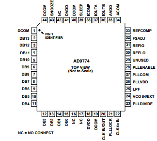
Pinouts:

AD9774 datasheet


Description

The AD9774 is a single supply, oversampling, 14-bit digital-to analog converter (DAC) optimized for waveform reconstruction applications requiring exceptional dynamic range. Manufactured on an advanced CMOS process, it integrates a complete, low distortion 14-bit DAC with a 4×digital interpolation filter and clock multiplier. The two-stage, 4×digital interpolation filter provides more than a six-fold reduction in the complexity of the analog reconstruction-filter. It does so by multiplying the input data rate by a factor of four while simultaneously suppressing the original inband images by more than 69 dB. The on-chip clock multiplier provides all the necessary clocks. The AD9774 can reconstruct full-scale waveforms having bandwidths as high as 13.5 MHz when operating at an input data rate of 32 MSPS and a DAC output rate of 128 MSPS. The 14-bit DAC provides differential current outputs to support differential or single-ended applications. A segmented current source architecture is combined with a proprietary switching technique to reduce spurious components and enhance dynamic performance. Matching between the two current outputs ensures enhanced dynamic performance in a differential output configuration. The differential current outputs may be fed into a transformer or tied directly to an output resistor to provide two complementary, single-ended voltage outputs. A differential op amp topology can also be used to obtain a single-ended output voltage. The output voltage compliance range is nominally 1.25 V.

Features

1. Single 3 V or 5 V Supply
2. 14-Bit DAC Resolution and Input Data Width
3. 32 MSPS Input Data Rate at 5 V
4. 13.5 MHz Reconstruction Bandwidth
5. 12 ENOBS @ 1 MHz
6. 77 dBc SFDR @ 5 MHz
7. 43 Interpolation Filter
8. 69 dB Image Rejection
9. 84% Passband to Nyquist Ratio
10. 0.002 dB Passband Ripple
11. 23 3/4 Cycle Latency
12. Internal 43Clock Multiplier
13. On-Chip 1.20 V Reference

Applications

1. Communication Transmit Channel:
2. Wireless Basestations
3. ADSL/HFC Modems
4. Direct Digital Synthesis (DDS)

Other data sheets are available within the file: AD9774AS, AD9774EB

AD9774 Datasheet PDF Download


AD9774 pdf