Part Number: AD9775
Function: 0.3-25V; 14-bit, 160MSPS 2x/4x/8x interpolating dual TxDAC+ D/A converter
Package: 80-lead, thin quad flat package, exposed pad (TQFP_EP) Type
Manufacturer: Analog Devices
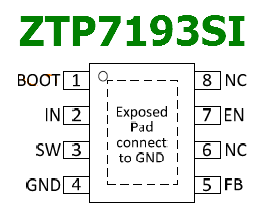
Pinouts:

Description
The AD9775 is the 14-bit member of the AD977x pin compatible, high performance, programmable 2×/4×/8× interpolating TxDAC+ family. The AD977x family features a serial port interface (SPI) that provides a high level of programmability, thus allowing for enhanced system-level options. These options include selectable 2×/4×/8× interpolation filters; fS/2, fS/4, or fS/8 digital quadrature modulation with image rejection; a direct IF mode; programmable channel gain and offset control; programmable internal clock divider; straight binary or twos complement data interface; and a single-port or dual-port data interface. The selectable 2×/4×/8× interpolation filters simplify the requirements of the reconstruction filters while simultaneously enhancing the pass-band noise/distortion performance of TxDAC+ devices. The independent channel gain and offset adjust registers allow the user to calibrate LO feedthrough and sideband suppression errors associated with analog quadrature modulators. The 6 dB of gain adjustment range can also be used to control the output power level of each DAC.
Features
1. 14-bit resolution, 160 MSPS/400 MSPS input/output data rate
2. Selectable 2×/4×/8× interpolating filter
3. Programmable channel gain and offset adjustment
4. fS/4, fS/8 digital quadrature modulation capability
5. Direct IF transmission mode for 70 MHz + IFs
6. Enables image rejection architecture
7. Fully compatible SPI® port
8. Excellent ac performance
9. SFDR: −71 dBc @ 2 MHz to 35 MHz
10. W-CDMA ACPR: −71 dB @ IF = 19.2 MHz
11. Internal PLL clock multiplier
12. Selectable internal clock divider
13. Versatile clock input
14. Differential/single-ended sine wave or TTL/CMOS/LVPECL compatible
15. Versatile input data interface
16. Twos complement/straight binary data coding
17. Dual-port or single-port interleaved input data
18. Single 3.3 V supply operation
19. Power dissipation: 1.2 W @ 3.3 V typical
20. On-chip, 1.2 V reference
Applications
1. Communications
2. Analog quadrature modulation architecture
3. 3G, multicarrier GSM, TDMA, CDMA systems
4. Broadband wireless, point-to-point microwave radios Instrumentation/ATE
Other data sheets are available within the file:
AD9775EB, AD9775BSV, AD9775BSVRL, AD9775BSVZ
AD9775 Datasheet PDF Download