H27UBG8T2CTR Datasheet – 32Gb MLC NAND Flash – SK Hynix

Part Number: H27UBG8T2CTR, H27UBG8T2CTR-BC

Function: 32Gb(4096M x 8bit) Legacy MLC NAND Flash Memory

Package: TSOP-48/SDP Type

Manufacturer: SK Hynix

Image :
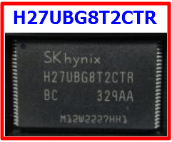
H27UBG8T2CTR nand flash memory

Description

OPERATING RANG : 2.7 to 3.6V

The product part NO.H27UBG8T2CTR-BC is a single 3.3V 32Gbit NAND flash memory. The Device contains 2 planes in a single die. Each plane is made up of the 1,044 blocks. Each block consists of 256 programmable pages. Each page contains 8,832 bytes. The pages are subdivided into an 8,192 byte main data storage area with a spare 640 byte district. Page program operation can be performed in typical 1,500us, and a single block can be erased in typical 5ms

Pinout
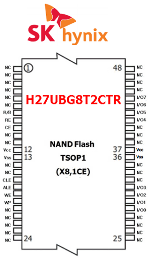
H27UBG8T2CTR datasheet pinout
Features

1. Multi Level Cell(MLC) Technology

2. NAND Interface
– x8 bus width
– Multiplexed address/data
– Pin-out compatibility for all densities

3. Supply Voltage
– Vcc = 2.7 V ~ 3.6 V

4. Organization
– Page size : 8832 (8192+640spare)bytes
– Block size : 256 pages (2M+160K)bytes
– Plane size : 1024 + 22 blocks
– Device size : 2048 + 44 Blocks

5. Page Read Time
– Random Read Time(tR) : 60us / 80 us (Typ. / Max.)
– Sequential Access(tRC/tWC) : 16ns (Min.)

6. Write Time
– Page program : 1500us(Typ.)

7. Block Erase Time
– Block erase : 5ms (Typ.)

8. Multi-Plane Architecture
– Two independent planes architecture
– Parallel operations on both planes available, effectively halving program, read and erase time


H27UBG8T2CTR Datasheet PDF


Related articles across the web

25L12835F Datasheet – 128Mb bits serial Flash memory – MXIC

Part Number: 25L12835F, 25L12835F

Function: 128Mb bits serial Flash memory, which is configured as 16,777,216 x 8 internally.

Package: 8-pin SOP(200mil), 16-pin SOP(300mil), 8-land WSON (6x5mm), 8-land WSON (8x6mm) Type

Manufacturer: Linkage ( Goston Electronics )

Image
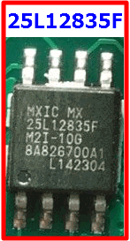
25L12835F flash memory

Description

MX25L12835F is 128Mb bits serial Flash memory, which is configured as 16,777,216 x 8 internally. When it is in two or four I/O mode, the structure becomes 67,108,864 bits x 2 or 33,554,432 bits x 4.

MX25L12835F feature a serial peripheral interface and software protocol allowing operation on a simple 3-wire bus while it is in single I/O mode. The three bus signals are a clock input (SCLK), a serial data input (SI), and a serial data output (SO). Serial access to the device is enabled by CS# input.

Pinouts

25L12835F datasheet pinout

Features

1. Serial Peripheral Interface compatible — Mode 0 and Mode 3

2. Single Power Supply Operation
– 2.7 to 3.6 volt for read, erase, and program operations

3. 128Mb: 134,217,728 x 1 bit structure or 67,108,864 x 2 bits (two I/O mode) structure or 33,554,432 x 4 bits (four I/O mode) structure

4. Protocol Support
– Single I/O, Dual I/O and Quad I/O

5. Latch-up protected to 100mAfrom -1V to Vcc +1V

6. Low Vcc write inhibit is from 2.3V to 2.5V

7. Fast read for SPI mode
– Support clock frequency up to 133MHz for all protocols
– Support Fast Read, 2READ, DREAD, 4READ, QREAD instructions.
– Configurable dummy cycle number for fast read operation

8. Quad Peripheral Interface (QPI) available

9. Equal Sectors with 4K byte each, or Equal Blocks with 32K byte each or Equal Blocks with 64K byte each
– Any Block can be erased individually

10. Programming :
– 256byte page buffer
– Quad Input/Output page program(4PP) to enhance program performance

11. Typical 100,000 erase/program cycles

12. 20 years data retention

25L12835F Datasheet PDF


Related articles across the web