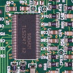
PS2251-07 Datasheet – USB 3.0-to-Flash Microcontroller Chip

Part Number: PS2251-07

Function:  Ultra-high-speed USB 3.0-to-Flash micro-controller chip

Package: TQFP64, EP-LQFP 48 Package

Manufacturer: Phison Electronics

Image:

PS2251-07 datasheet usb controller

Description

Phison PS2251-07, an ultra-high-speed USB-to-Flash micro-controller chip, supports 3X/2X/1X nm flash memory. PS2251-07 is backward compatible with USB 2.0 and USB 1.1.

1. Controllor Highlights
– Support USB 3.1 GEN1 interface
– Backward complies with USB 2.0 & 1.1 host interface specification
– Built-in enhanced of ECC circuit (the BCH)
– Support Super Speed ​​(5Gb / s)
– Support High Speed ​​(480Mb / s), Full Speed ​​(12Mb / s)

2. Characteristics
– Using the Program RAM (firmware update)
– Available in a TQFP64, EP-LQFP 48 package
– Applied voltage: 4.5V ~ 5.5V
– Built-in regulator support the 3.3V/1.8V flash memory I / O interface

3. Support interface
– USB 3.1 GEN1

4. NAND flash memory support
– Support 3X / 2X / 1X NAND flash memory
– Support SLC / MLC / TLC flash memory
– Support the Open NAND Flash Interface 3 (ONFI 3)
– Support of Toggle 2.0 mode DDR flash memory

5. Other Features
– Support Dynamic/ Static Wear-Leveling
– Power Saving implemented
– Supports multiple partitions and hidden mode


Reference site : http://www.usbdev.ru/f/index.php?topic=1892.0

PS2251-07 Datasheet

PS2251-33 pdf


Related articles across the web

Other data sheets are available within the file: PS2251
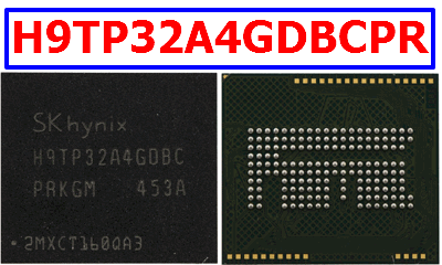
H9TP32A4GDBCPR Datasheet – 4GB eNAND (x8) Flash Memory

Part Number: H9TP32A4GDBCPR, H9TP32A4GDBCPR-KGM

Function: 4GB eNAND (x8) / LPDDR2-S4B 4Gb(x32) / Flash Memory

Package: 162-ball FBGA – 11.5×13.0mm2, 1.0t, 0.5mm pitch

Manufacturer: Hynix Semiconductor

Images:

H9TP32A4GDBCPR datasheet memory

Description

The SK hynix e‐NAND is an embedded flash memory storage solution. The SK hynix e‐NAND was developed for universal low cost data storage and communication media. The SK hynix e‐NAND is fully compatible with MMC bus and host.
The SK hynix e‐NAND communications are made through an advanced 13‐pin bus, and it can be either 1‐bit, 4‐bit, or 8‐bit in width. The SK hynix e‐NAND operates in high‐speed mode at clock frequencies equal or higher than 20MHz as defined in the MMC JEDEC standard. The communication protocol is defined in this MMC JEDEC standard.
The SK hynix e‐NAND is designed to cover a wide area of applications such as smart phones, cameras, organizers, PDA, digital recorders, MP3 players, pagers, electronic toys, etc. Features are mainly high speed performance, low power consumption, low cost and high density.

[…]

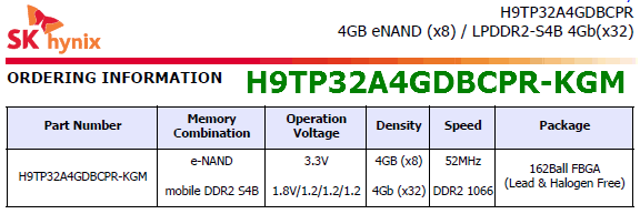
Ordering Information

H9TP32A4GDBCPR-KGM Ordering information

[ e-NAND ]

1. Packaged NAND flash memory with MultiMedia-Card interface
2. e-NAND system specification, compliant with V4.41
3. Full backward compatibility with previous e-NAND system specification
4. Bus mode
– High-speed eMMC protocol.
– Three different data bus widths : 1 bit, 4 bits,8 bits.
– Data transfer rate: up to 104Mbyte/s
– DDR mode supported

[ LPDDR2 S4B ]

1. Programmable RL (Read Latency) and WL (Write Latency)
2. Programmable burst length: 4, 8 and 16
3. Auto refresh and self refresh supported
4. All bank auto refresh and per bank auto refresh supported
5. Auto TCSR (Temperature Compensated Self Refresh)
6. PASR (Partial Array Self Refresh) by Bank Mask and Segment Mask

Pinout

H9TP32A4GDBCPR pinout


H9TP32A4GDBCPR Datasheet