V400HJ6-PE1 Datasheet PDF – 40 inch TFT LCD Module

This is TFT LCD Module.

Part Number: V400HJ6-PE1, V400HJ6PE1

Function: 40” TFT Liquid Crystal Display

Active Area : 878.112 (H) x 485.352 (V) mm

Manufacturer: InnoLux

Image

V400HJ6-PE1 TFT LCD datasheet

Description

V400HJ6-PE1 is a 40” TFT Liquid Crystal Display product with driver ICs and 2ch-LVDS interface. This product supports 1920 x 1080 Full HDTV format and can display 16.7M colors (8-bit). The backlight unit is not built in.

V400HJ6-PE1 Pinout

V400HJ6-PE1 TFT LCD datasheet

1 NC No connection (2)
2 SCL I2C clock (For Vcom tunning)
3 SDA I2C data (For Vcom tunning)
4 NC No connection
5 NC No connection
6 NC No connection
7 SELLVDS LVDS data format Selection (3)(4)
8 NC No Connection
9 NC No Connection
10 NC No connection
11 GND Ground
12 ORX0- Odd pixel Negative LVDS differential data input. Channel 0
13 ORX0+ Odd pixel Positive LVDS differential data input. Channel 0
14 ORX1- Odd pixel Negative LVDS differential data input. Channel 1
15 ORX1+ Odd pixel Positive LVDS differential data input. Channel 1
16 ORX2- Odd pixel Negative LVDS differential data input. Channel 2
17 ORX2+ Odd pixel Positive LVDS differential data input. Channel 2
18 GND Ground
19 OCLK- Odd pixel Negative LVDS differential clock input.
20 OCLK+ Odd pixel Positive LVDS differential clock input.
21 GND Ground
22 ORX3- Odd pixel Negative LVDS differential data input. Channel 3
23 ORX3+ Odd pixel Positive LVDS differential data input. Channel 3
24 N.C. No Connection
25 N.C. No Connection
26 GND Ground
27 GND Ground
28 ERX0- Even pixel Negative LVDS differential data input. Channel 0
29 ERX0+ Even pixel Positive LVDS differential data input. Channel 0
30 ERX1- Even pixel Negative LVDS differential data input. Channel 1
31 ERX1+ Even pixel Positive LVDS differential data input. Channel 1
32 ERX2- Even pixel Negative LVDS differential data input. Channel 2
33 ERX2+ Even pixel Positive LVDS differential data input. Channel 2
34 GND Ground
35 ECLK- Even pixel Negative LVDS differential clock input
36 ECLK+ Even pixel Positive LVDS differential clock input
37 GND Ground
38 ERX3- Even pixel Negative LVDS differential data input. Channel 3
39 ERX3+ Even pixel Positive LVDS differential data input. Channel 3
40 N.C. No Connection (2)
41 N.C. No Connection (2)
42 GND Ground
43 GND Ground
44 GND Ground
45 GND Ground
46 GND Ground47 N.C. No Connection (2)
48 VCC Power input (+12V)
49 VCC Power input (+12V)
50 VCC Power input (+12V)
51 VCC Power input (+12V)

SPECIFICATIONS

1. Screen Diagonal [in] 40”
2. Pixels [lines] 1920 × R.G.B × 1080
3. Active Area [mm] 878.112 (H) x 485.352 (V)
4. Sub-Pixel Pitch [mm] 0.15245 (H) x 0.4494 (V)
5. Pixel Arrangement RGB Vertical Stripe
6. Weight [g] 1350 Typ. (g)
7. Physical Size [mm] 888.392 x 494.152
8. Display Mode Transmissive Mode / Normallly Black
9. Contrast Ratio : Typ.5000:1 (Typical value measure by INX’s Module)
10. Glass thickness (Array / CF) [mm] 0.5 / 0.5


V400HJ6-PE1 Datasheet


Related articles across the web

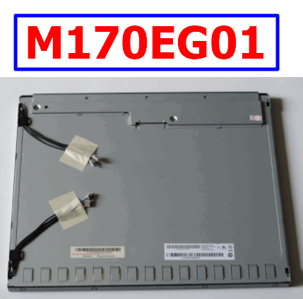
M170EG01 Datasheet – 17 Inch, Color TFT-LCD Module

Part Number: M170EG01

Function: 17 Inch, Color TFT-LCD Module

Physical Size (H x V x D) : 358.5(H) x 296.5(V) Typ. x 15.8(D) Max [mm]

Manufacturer: Auo ( AU Optronics )

Image

M170EG01 datasheet LCD

Description

This specification applies to the 17 inch Color TFT-LCD Module M170EG01.

The display supports the W SXGA+ (1280(H) x 1024(V)) screen format and 16.7M colors (RGB 6-bits+Hi-RFC data). All input signals are 2 Channel LVDS interface compatible. This module does not contain an inverter card for backlight.

Display Characteristics :

1. Screen Diagonal [mm] : 432 (17.0”)

2. Active Area [mm] : 337.920(H) × 270.336(V)

3. Pixels H x V : 1280 × 3(RGB) × 1024

4. Pixel Pitch [mm] : 0.264(per one triad) × 0.264

5. Pixel Arrangement : R.G.B. Vertical Stripe

6. Display Mode : Normally White

7. White Luminance [cd/m2] : 650 (center,Typ)@7.5 mA

8. Contrast Ratio : 800 : 1 (Typ)

9. Power Consumption [Watt] : 25.8 W (Typ)

10. Weight [Grams] : 2100 Max.

Pinouts:

The module using a pair of LVDS receiver SN75LVDS82(Texas Instruments) or compatible. LVDS is a
differential signal technology for LCD interface and high speed data transfer device. Transmitter shall be SN75LVDS83(negative edge sampling) or compatible. The first LVDS port(RxOxxx) transmits odd pixels while the second LVDS port(RxExxx) transmits even pixels.

1 RxO0- Negative LVDS differential data input (Odd data)
2 RxO0+ Positive LVDS differential data input (Odd data)
3 RxO1- Negative LVDS differential data input (Odd data)
4 RxO1+ Positive LVDS differential data input (Odd data)
5 RxO2- Negative LVDS di fferential data input (Odd data, H -Sync,V-Sync,DSPTMG)
6 RxO2+ Positive LVDS differential data input (Odd data, H -Sync,V-Sync,DSPTMG)
7 GND Power Ground
8 RxOC- Negative LVDS differential clock input (Odd clock)
9 RxOC+ Positive LVDS differential clock input (Odd clock)
10 RxO3- Negative LVDS differential data input (Odd data)
11 RxO3+ Positive LVDS differential data input (Odd data)
12 RxE0- Negative LVDS differential data input (Even clock)
13 RxE0+ Positive LVDS differential data input (Even data )
14 GND Power Ground
15 RxE1- Positive LVDS differential data input (Even data)
16 RxE1+ Negative LVDS differential data input (Even data)
17 GND Power Ground
18 RxE2- Negative LVDS differential data input (Even data)
19 RxE2+ Positive LVDS differential data input (Even data)
20 RxEC- Negative LVDS differential clock input (Even clock)
21 RxEC+ Positive LVDS differential clock input (Even clock)
22 RxE3- Negative LVDS differential data input (Even data)
23 RxE3+ Positive LVDS differential data in put (Even data)
24 GND Power Ground
25 GND Power Ground
26 NC No contact (For AUO test only)
27 GND Power Ground
28 VCC +5.0V Power Supply
29 VCC +5.0V Power Supply
30 VCC +5.0V Power Supply


Other data sheets are available within the file: M170EG-01

M170EG01 Datasheet PDF Download

 M170EG01 pinout


Related articles across the web