HMD1M32M2GL Datasheet PDF – 1M x 32 bits Dynamic RAM Module

Part Number: HMD1M32M2GL

Function: 4Mbyte(1Mx32) Dynamic RAM, 1K Refresh, 72 Pin SIMM, 5V

Package: 72 Pin Single-in-line Module type

Manufacturer: Hanbit ( www.hbe.co.kr )

Images :
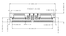
HMD1M32M2GL datasheet


Description

The HMD1M32M2GL is an 1M x 32 bits Dynamic RAM MODULE which is assembled 2 pieces of 1M x 16bit DRAMs in 42 pin SOJ package on single sides the printed circuit board with decoupling capacitors. The HMD1M32M2GL is optimized for application to the systems, which are required high density and large capacity such as main memory of the computers and an image memory systems, and to the others, which are, requested compact size.

Features

1. Fast Page Mode Capability
2. Single +5V± 0.5V power supply
3. All inputs and outputs TTL Compatible
4. 1,024 Refresh Cycles/16ms
5. Low Power

Other data sheets are available within the file: HMD1M32M2, HMD1M32M2G-5, HMD1M32M2G-6

HMD1M32M2GL Datasheet PDF Download


HMD1M32M2GL pdf

K9F1G08U0E Datasheet – 1Gb E-die NAND Flash Memory – Toshiba

Part Number: K9F1G08U0E, K9F1G08U0E-S

Function: 1Gb E-die NAND Flash, Single-Level-Cell (1bit/cell)

Package: 48 Pin TSSOP,  TSOP1, 63FBGA Pin Type

Manufacturer: Samsung

Image

K9F1G08U0E nand flash memory

General Description

Offered in 128Mx8bit, the K9F1G08U0E is a 1G-bit NAND Flash Memory with spare 32M-bit. Its NAND cell provides the most cost-effective solution for the solid state application market. A program operation can be performed in typical 400s on the (2K+64)Byte page and an erase operation can be performed in typical 4.5ms on a (128K+4K)Byte block. Data in the data register can be read out at 25ns cycle time per Byte.

The I/O pins serve as the ports for address and data input/output as well as command input. The on-chip write controller automates all program and erase functions including pulse repetition, where required, and internal verification and margining of data. Even the write-intensive systems can take advantage of the K9F1G08U0E extended reliability by providing ECC(Error Correcting Code) with real time mapping-out algorithm. The K9F1G08U0E is an optimum solution for large nonvolatile storage applications such as solid state file storage and other portable applications requiring non-volatility.


Pinout

K9F1G08U0E datasheet pinout
Features

1. Voltage Supply
– 3.3V Device(K9F1G08U0E) : 2.7V ~ 3.6V

2. Organization
– Memory Cell Array : (128M + 4M) x 8bit
– Data Register : (2K + 64) x 8bit

3. Automatic Program and Erase
– Page Program : (2K + 64)Byte
– Block Erase : (128K + 4K)Byte

4. Page Read Operation
– Page Size : (2K + 64)Byte
– Random Read : 40s(Max.)
– Serial Access : 25ns(Min.)


K9F1G08U0E Datasheet


Related articles across the web