TC58TEG6DCJTA00 Datasheet – NAND Memory – Toshiba

Part Number: TC58TEG6DCJTA00

Function: NAND memory, Toggle DDR1.0

Package: 48 Pin Type

Manufacturer: Toshiba

Image
TC58TEG6DCJTA00

General Description

Toggle DDR is a NAND interface for high performance applications which support data read and write operations using bidirectional DQS. Toggle DDR NAND has implemented ’Double Data Rate’ without a clock. It is compatible with functions and command which have been supported in conventional type NAND(i.e. SDR NAND) while providing high data transfer rate based on the high-speed Toggle DDR Interface and saving power with separated DQ voltage. For applications that require high capacity and high performance NAND, Toggle DDR NAND is the most appropriate.

Product Organization :

TC58TEG6DCJTA00 datasheet


Toggle DDR1.0 NAND supports the interface speed of up to 100 MHz, which is faster than the data transfer rate offered by SDR NAND. Toggle DDR NAND transfers data at high speed using DQS signal that behaves as a clock, and DQS shall be used only when data is transferred for optimal power consumption.

This device supports both SDR interface and Toggle DDR interface. When starting, the device is activated in SDR mode. The interface mode can be changed into Toggle DDR interface utilizing specific command issued by the Host.

Pinout

TC58TEG6DCJTA00 pinout


TC58TEG6DCJTA00 Datasheet


Related articles across the web

PSD913F2-90M Datasheet PDF – Flash ISP Peripherals

Part Number: PSD913F2-90M

Function: Flash in-system programmable (ISP) peripherals for 8-bit MCUs, 90ns

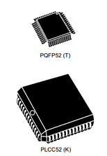
Package: PQFP 52, PLCC 52 Pin Type

Manufacturer: STMicroelectronics

Images :

PSD913F2-90M datasheet

Description

The PSD913F2-90M family of Programmable System Devices (for 8-bit microcontrollers) brings In-System-Programmability (ISP) to Flash memory and programmable logic.The result is a simple and flexible solution for embedded designs. PSD9XX devices combine many of the peripheral functions found in MCU based applications :

1. Up to 2 Mbit of Flash memory

2. A secondary 256 Kbit Flash memory

3. Over 2,000 gates of Flash programmable logic

4. Up to 256 Kbit SRAM

5. Reconfigurable I/O ports

6. Programmable power management.

Features

1. Single Supply Voltage:
(1) 5 V±10% for PSD9xxF2
(2) 3.3 V±10% for PSD9xxF2-V

2. Up to 2Mbit of Primary Flash Memory (8 uniform sectors)

3. 256Kbit Secondary Flash Memory (4 uniform sectors)

4. Up to 256Kbit SRAM

5. Over 2,000 Gates of PLD: DPLD

6. 27 Reconfigurable I/O ports

7. Enhanced JTAG Serial Port

8. Programmable power management

9. High Endurance:
(1) 100,000 Erase/Write Cycles of Flash Memory
(2) 1,000 Erase/Write Cycles of PLD

Other data sheets are available within the file: PSD913, PSD913F, PSD913F2, PSD913F2-70J,

PSD913F2-70M, PSD934F2, PSD954F2, PSD934F2-90M, PSD954F2V-90M

PSD913F2-90M Datasheet PDF Download


PSD913F2-90M pdf