Part Number: H26M11001BAR
Function : 1GB e-NAND Memory
Package: 169-FBGA (12x16x1.3) Type
Manufacturer: Hynix
Image

Description
The H26M11001BAR is 1GB e-NAND Memory.
The Hynix e-NAND Module is a very small, flash storage device, designed specifically for storage applications that put a premium on small form factor, low power and low cost. Flash is the ideal storage medium for portable, battery-powered devices. It features lowpower consumption and is non-volatile, requiring no power to maintain the stored data. It also has a wide operating range for temperature, shock and vibration.e-NAND is well-suited to meet the needs of small, low power, electronic devices. e-NAND is expected to be used in a wide variety of portable devices like mobile
phones, PMP, Smart phones, PDA, Media Players and etc.
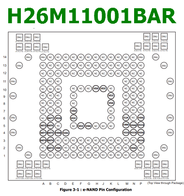
Pinout
Features
1. JEDEC JESD84 V4.3 compatible
2. Backward compatible with earlier JESD84
3. Maximum data rate with up to 52MB/sec interface speed ( using 8 parallel data lines )
4. e-NAND supported clock frequencies 0~20MHz, 0~26MHz, 0~52MHz
5. e-NAND support for three different data bus width modes: 1bit(default), 4bit and 8 bit
6. Correction of memory field errors
7. Simple erase mechanism
8. Password Protection of e-NAND
Other data sheets are available within the file: H26M11001
H26M11001BAR Datasheet PDF