AR9344 Datasheet PDF – IEEE 802.11n 2×2 2.4/5 GHz SoC

Part Number: AR9344

Function: Feature-Rich IEEE 802.11n 2×2 2.4/5 GHz Premium SoC

Package: BGA-409

Manufacturer: Atheros

This post explains for the System-on-a-Chip (SoC).

Image :
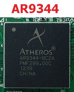
AR9344 image

Description

The Atheros AR9344 is a highly integrated and feature-rich IEEE 802.11n 2×2 2.4/5 GHz System on-a-Chip (SoC) for advanced WLAN platforms.

It includes a MIPS 74Kc processor, PCI Express 1.1 Root Complex and Endpoint interfaces, five port IEEE 802.3 Fast Ethernet Switch with MAC/PHY, one MII/RMII/RGMII interface, one USB 2.0 MAC/PHY, and external memory interface for serial Flash, SDRAM, DDR1 or DDR2, I2S/SPDIF-Out audio interface, SLIC VOIP/PCM interface, two UARTs, and GPIOs that can be used for LED controls or other general purpose interface configurations.

Block Diagram :
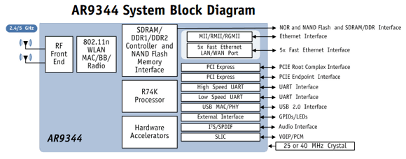
AR9344 datasheet block diagram

Features

1. 74Kc MIPS processor with 64 KB I-Cache and 32 KB D-Cache, operating at up to 533 MHz

2. External 16- or 32-bit DDR1, DDR2 operating at up to 200 MHz (400 M transfers/sec), or 16-
bit SDRAM memory interface operating at up to 200 MHz

3. NAND and SPI NOR Flash memory support

4. 10/100 Ethernet Switch with five IEEE 802.3 Ethernet LAN ports

5. MII/RMII/RGMII interface

AR9344 Datasheet PDF Download


Related articles across the web

TDA8375A Datasheet PDF – PAL/NTSC and NTSC TV Processor

Part Number: TDA8375A

Function: I2C-bus Controlled Economy PAL/NTSC and NTSC TV-processor

Package:  DIP 56 Pin Type

Manufacturer: Philips Semiconductor, NXP

Images:
TDA8375A datasheet processor

Description

The TDA8375A is I2C-bus controlled single-chip TV processor.

The various versions of the TDA837x series are I2C-bus controlled single-chip TV processors which are intended to be applied in PAL/NTSC (TDA8374 and TDA8375) and NTSC (TDA8373 and TDA8377) television receivers.

Features

1. Vision IF amplifier with high sensitivity and good figures for differential phase and gain

2. PLL demodulator for the IF signal

3. Alignment-free sound demodulator

4. Flexible source selection with a CVBS input for the internal signal and Y/C or CVBS input for the external signal

5. Audio switch

6. The output signal of the CVBS (Y/C) switch is externally available

7. Luminance delay line integrated

8. Slow start and slow stop of the horizontal drive pulses

Pinout:

TDA8375A pinout

Synchronization circuit

The sync separator is preceded by a controlled amplifier which adjusts the sync pulse amplitude to a fixed level. These pulses are fed to the slicing stage which operates at 50% of the amplitude.

Other data sheets are available within the file: TDA8375, TDA8373, TDA8373B, TDA8373A, TDA8374A

TDA8375A Datasheet PDF


TDA8375A pdf

Related articles across the web