SN74AHC595 Datasheet PDF – 8-Bit Shift Register

Part Number: SN74AHC595

Function: 8-BIT SHIFT REGISTERS WITH 3-STATE OUTPUT REGISTERS

Package: DIP, SOIC, SSOP 16 Pin Type

Manufacturer: Texas Instruments

Pinouts:

SN74AHC595 datasheet


Description

The SN74AHC595 device contains an 8-bit serial-in, parallel-out shift register that feeds an 8-bit D-type storage register. The storage register has parallel 3-state outputs. Separate clocks are provided for both the shift and storage registers. The shift register has a direct overriding clear (SRCLR) input, a serial (SER) input, and a serial output for cascading. When the output-enable (OE) input is high, all outputs except QH′ are in the high-impedance state.

Features

• Operating Range 2-V to 5.5-V Vcc

• 8-Bit Serial-In, Parallel-Out Shift

• Latch-Up Performance Exceeds 100 mA Per JESD 78, Class II

• ESD Protection Exceeds JESD 22

(1) 2000-V Human-Body Model (A114-A)
(2) 200-V Machine Model (A115-A)
(3) 1000-V Charged-Device Model (C101)


SN74AHC595 Datasheet PDF Download


SN74AHC595 pdf

Other data sheets are available within the file:

74AHC595D, 74AHC595DBR, 74AHC595DBRE4,

74AHC595DBRG4, 74AHC595DE4
SSTV16857 Datasheet – 14-Bit Registered Buffer

Part Number: SSTV16857

Function: 14-bit SSTL_2 registered driver with differential clock inputs

Package: TSSOP-48, TVSOP-48 and 56 ball VFBGA Type

Manufacturer: Philips Electronics ( https://www.nxp.com/ )

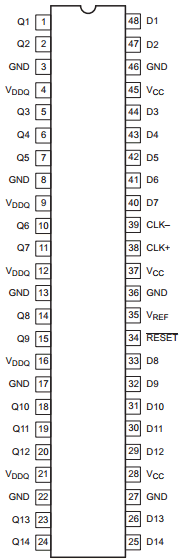
Pinouts:

SSTV16857 datasheet


Description

The SSTV16857 is a 14-bit SSTL_2 registered driver with differential clock inputs, designed to operate between 2.3 V and 2.7 V. VDDQ must not exceed VCC. Inputs are SSTL_2 type with VREFnormally at 0.5*VDDQ. The outputs support class I which can be used for standard stub-series applications or capacitive loads. Master reset (RESET) asynchronously resets all registers to zero. The SSTV16857 is intended to be incorporated into standard DIMM (Dual In-Line Memory Module) designs defined by JEDEC, such as DDR (Double Data Rate) SDRAM or SDRAM II Memory Modules. Different from traditional SDRAM, DDR SDRAM transfers data on both clock edges (rising and falling), thus doubling the peak bus bandwidth. A DDR DRAM rated at 133 MHz will have a burst rate of 266 MHz. The modules require between 23 and 27 registered control and address lines, so two 14-bit wide devices will be used on each module. The SSTV16857 is intended to be used for SSTL_2 input and output signals.

Features

• Stub-series terminated logic for 2.5 V VDDQ(SSTL_2)
• Optimized for DDR (Double Data Rate) SDRAM applications
• Inputs compatible with JESD8–9 SSTL_2 specifications.
• Flow-through architecture optimizes PCB layout
• ESD classification testing is done to JEDEC Standard JESD22.
• Protection exceeds 2000 V to HBM per method A114.
• Latch-up testing is done to JEDEC Standard JESD78, which exceeds 100 mA.
• Same form, fit, and function as SSTL16877
• Full DDR 200/266 solution @ 2.5 V when used with PCKV857
• See SSTV16856 for driver/buffer version with mode select.

Other data sheets are available within the file:

SSTV16857DGG, SSTV16857DGV, SSTV16857EV


SSTV16857 Datasheet PDF Download


SSTV16857 pdf