Part Number: SN74ALVC244-EP
Marking : VA244IEP
Function: OCTAL BUFFER/DRIVER WITH 3-STATE OUTPUTS
Package: TSSOP 20 Pin Type
Manufacturer: Texas Instruments
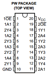
Pinouts:
Description
This octal buffer/line driver is designed for 1.65-V to 3.6-V VCCoperation. The SN74ALVC244 is organized as two 4-bit line drivers with separate output-enable (OE) inputs. When OE is low, the device passes data from the A inputs to the Y outputs. When OE is high, the outputs are in the
high-impedance state. To ensure the high-impedance state during power up or power down, OE shall be tied to VCC through a pullup resistor; the minimum value of the resistor is determined by the current-sinking capability of the driver.
Features
• Controlled Baseline
– One Assembly/Test Site, One Fabrication Site
• Enhanced Diminishing Manufacturing Sources (DMS) Support
• Enhanced Product-Change Notification
• Qualification Pedigree
• Operates From 1.65-V to 3.6-V VCC
• Max tpd of 2.8 ns at 3.3-V VCC
• ±24-mA Output Drive at 3.3-V VCC
• Latch-Up Performance Exceeds 250 mA PerJESD 17
• ESD Protection Exceeds JESD 22
(1) 2000-V Human-Body Model (A114-A)
(2) 200-V Machine Model (A115-A)
(3) 1000-V Charged-Device Model (C101)
SN74ALVC244-EP Datasheet PDF Download


Other data sheets are available within the file:
SN74ALVC244EP, SN74ALVC244IPWREP, 74ALVC244, SN74ALVC244