MC74VHCT125A Datasheet PDF – Quad Bus Buffer

Part Number: MC74VHCT125A

Function: Quad Bus Buffer with 3-State Control Inputs

Manufacturer: ON Semiconductor

Pinouts:

MC74VHCT125A datasheet

Description

The MC74VHCT125A is a high speed CMOS quad bus buffer fabricated with silicon gate CMOS technology. It achieves high speed operation similar to equivalent Bipolar Schottky TTL while maintaining CMOS low power dissipation.

The device requires the 3−state control input (OE) to be set High to place the output into the high impedance state. The VHCT inputs are compatible with TTL levels. This device can
be used as a level converter for interfacing 3.3 V to 5.0 V, because it has full 5.0 V CMOS level output swings.

Features

1. High Speed: tPD = 3.8ns (Typ) at VCC = 5 V

2. Low Power Dissipation: ICC = 4 µA (Max) at TA = 25°C

3. High Noise Immunity: VNIH = VNIL = 28% VCC

4. Power Down Protection Provided on Inputs

5. Balanced Propagation Delays

6. Designed for 2 V to 5.5 V Operating Range

7. Low Noise: VOLP = 0.8 V (Max)


MC74VHCT125A Datasheet PDF Download


MC74VHCT125A pdf

Other data sheets are available within the file:

MC74VHCT125, MC74VHCT125AD, MC74VHCT125ADR2G,

MC74VHCT125ADT, MC74VHCT125ADTR2
SN74ALVC244-EP Datasheet PDF – 8-ch, 1.65-V to 3.6-V Buffer

Part Number: SN74ALVC244-EP

Marking : VA244IEP

Function: OCTAL BUFFER/DRIVER WITH 3-STATE OUTPUTS

Package: TSSOP 20 Pin Type

Manufacturer: Texas Instruments

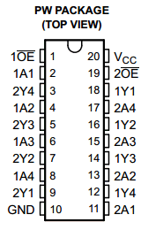
Pinouts:

SN74ALVC244-EP datasheet


Description

This octal buffer/line driver is designed for 1.65-V to 3.6-V VCCoperation. The SN74ALVC244 is organized as two 4-bit line drivers with separate output-enable (OE) inputs. When OE is low, the device passes data from the A inputs to the Y outputs. When OE is high, the outputs are in the
high-impedance state. To ensure the high-impedance state during power up or power down, OE shall be tied to VCC through a pullup resistor; the minimum value of the resistor is determined by the current-sinking capability of the driver.

Features

• Controlled Baseline
– One Assembly/Test Site, One Fabrication Site

• Enhanced Diminishing Manufacturing Sources (DMS) Support

• Enhanced Product-Change Notification

• Qualification Pedigree

• Operates From 1.65-V to 3.6-V VCC

• Max tpd of 2.8 ns at 3.3-V VCC

• ±24-mA Output Drive at 3.3-V VCC

• Latch-Up Performance Exceeds 250 mA PerJESD 17

• ESD Protection Exceeds JESD 22

(1) 2000-V Human-Body Model (A114-A)
(2) 200-V Machine Model (A115-A)
(3) 1000-V Charged-Device Model (C101)


SN74ALVC244-EP Datasheet PDF Download


SN74ALVC244-EP pdf

Other data sheets are available within the file:

SN74ALVC244EP, SN74ALVC244IPWREP, 74ALVC244, SN74ALVC244