DAC38J84 Datasheet PDF – Quad-Channel, 16-Bit, DAC

Part Number: DAC38J84

Function: Quad-Channel, 16-Bit, 1.6/2.5 GSPS, DAC with JESD204B Interface

Package: FCBGA (144) Type

Manufacturer: Texas Instruments

Image and Pinouts:

DAC38J84 datasheet


Description

The terminal-compatible DAC37J84, DAC38J84 family is a low power, 16-bit, quad-channel, 1.6/2.5 GSPS digital to analog converter (DAC) with JESD204B interface.

Digital data is input to the device through 1, 2, 4 or 8 configurable serial JESD204B lanes running up to 12.5 Gbps with on-chip termination and programmable equalization. The interface allows JESD204B Subclass 1 SYSREF based deterministic latency and full synchronization of multiple devices.

The device includes features that simplify the design of complex transmit architectures. Fully bypassable 2x to 16x digital interpolation filters with over 90 dB of stop-band attenuation simplify the data interface and reconstruction filters. An on-chip 48-bit Numerically Controlled Oscillator (NCO) and independent complex mixers allow flexible and accurate carrier placement.

A high-performance low jitter PLL simplifies clocking of the device without significant impact on the dynamic range. The digital Quadrature Modulator Correction (QMC) and Group Delay Correction (QDC) enable complete IQ compensation for gain, offset, phase, and group delay between channels in direct up-conversion applications. A programmable Power Amplifier (PA) protection mechanism is available to provide PA protection in cases when the abnormal
power behavior of the input data is detected.

Official Homepage: https://www.ti.com/product/dac38j84

Other data sheets are available within the file:

DAC37J84IAAV, DAC37J84IAAVR, DAC38J84IAAV, DAC38J84IAAVR


DAC38J84 Datasheet PDF Download


DAC38J84 pdf

TPS51367 Datasheet PDF – Integrated FET Converter

Part Number: TPS51367, TPS51367RVET, TPS51367RVER

Function: Integrated FET Converter

Package: VQFN-CLIP 28 Pin

Manufacturer: Texas Instruments

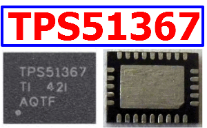
Image:

TPS51367 datasheet fet converter

Description

This is synchronous buck converter with ultra-low quiescent current.

The TPS51367 is a high-voltage input, synchronous converter with integrated FET, based on DCAP-2 control topology, which enables fast transient response and supports both POSCAP and all MLCC output capacitors. TI proprietary FET technology combined with TI leading-edge package technology provides the highest density solution for single-output power rail such as VCCIO and VDDQ for DDR notebook memory, or any point-of-load (POL) in wide application.

The key feature of the device is its ULQ Mode to enable low-bias current (100 µA in low power mode, enabled by LP#). This feature is extremely beneficial for long battery life in system standby mode.

The feature set includes switching frequency of 800 kHz. Programmable soft-start time with an external capacitor. auto skip, pre-bias startup, integrated bootstrap switch, power good, enable and a full suite of fault protection schemes, including OCL, UVP, OVP, 5-V UVLO and thermal shutdown.

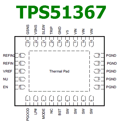
Pinout

TPS51367 pinout


Features

1. Input Voltage Range: 3 V to 22 V

2. Output Voltage Range: 0.6 V to 2 V

3. 12-A Integrated FET Converter

4. Fewest External Components

5. ULQ-100 Mode of Operation to Enable Long Battery Life During System Standby

6. Soft-Start Time Programmable by External Capacitor

7. Switching Frequency: 400 kHz and 800 kHz

8. D-CAP2 Architecture to Enable POSCAP and All MLCC Output Capacitor Usage

9. Integrated and Temperature Compensated Low-Side On-Resistance Sensing for Accurate OCL Protection

10. Powergood Output OCL, OVP, UVP and UVLO Protections

11. Thermal Shutdown (non-latch)

12. Output Discharge Function

13. Integrated Boost MOSFET Switch

Official Homepage: https://www.ti.com/product/TPS51367

TPS51367 Datasheet

Related articles across the web