LF353 Datasheet – JFET-Input Dual Operational Amplifier

Part Number: LF353

Function: JFET-INPUT DUAL OPERATIONAL AMPLIFIER

Package: DIP 8 or SOP 8 Pin

Manufacturer: Texas Instruments

Image
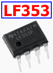
LF353 Operational Amplifier

Description

This device is a low-cost, high-speed, JFET-input operational amplifier with very low input offset voltage. It requires low supply current yet maintains a large gain-bandwidth product and a fast slew rate. In addition, the matched high-voltage JFET input provides very low input bias and offset currents.
The LF353 can be used in applications such as high-speed integrators, digital-to-analog converters, sample-and-hold circuits, and many other circuits. The LF353 is characterized for operation from 0°C to 70°C.

Pinouts:
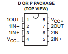
LF353 datasheet


Features

1. Low Input Bias Current 50 pA Typical
2. Low Input Noise Current 0.01 pA/√Hz Typical
3. Low Supply Current 3.6 mA Typical
4. High Input Impedance 1012 Ω Typical
5. Internally-Trimmed Offset Voltage
6. Gain Bandwidth 3 MHz Typical
7. High Slew Rate 13 V/µs Typical


LF353 Datasheet PDF Download


LF353 pdf

Other data sheets are available within the file:  LF353D, LF353DE4, LF353DG4, LF353DR

Related articles across the web

TL074 Datasheet – JFET-Input Operational Amplifier – TI

Part Number: TL074, TL074CN

Function : LOW-NOISE JFET-INPUT OPERATIONAL AMPLIFIERS

Package: PDIP, SOIC 14 Pin Type

Manufacturer: Texas Instruments

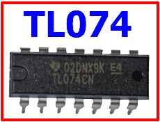
Image

tl074-jfet-operational-amplifier

Description

The TL07xx, TL074 JFET-input operational amplifier family is designed to offer a wider previously developed operational amplifier family. Each of these JFET-input operational amplifiers incorporates well-matched, high-voltage JFET and bipolar transistors in a monolithic integrated circuit. The devices feature high slew rates, low-input bias and offset currents, and low offset-voltage temperature coefficient. The low harmonic distortion and low noise make the TL07xseries ideally suited for high-fidelity and audio pre-amplifier applications. Offset adjustment and external compensation options are available within the TL07x family.


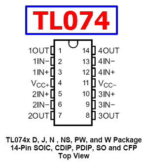
Pinout

tl074-datasheet-pinout


Features

1. Low Power Consumption
2. Wide Common-Mode and Differential Voltage Ranges
3. Low Input Bias and Offset Currents
4. Output Short-Circuit Protection
5. Low Total Harmonic Distortion: 0.003% Typical
6. Low Noise Vn = 18 nV/√Hz Typ at f = 1 kHz
7. High-Input Impedance: JFET Input Stage
8. Internal Frequency Compensation
9. Latch-Up-Free Operation
10. High Slew Rate: 13 V/μs Typical
11. Common-Mode Input Voltage Range ncludes VCC+


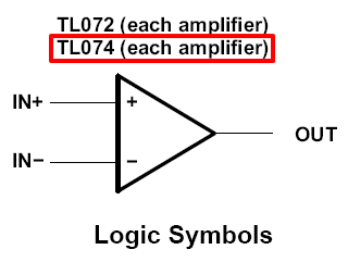
Logic Symbols

tl074-logic-symbols


Official Homepage: https://www.ti.com/product/TL074

TL074 Datasheet


Related articles across the web