SM4109 Datasheet PDF – Screen LCD Chip IC – QFN 40 Pin

Part Number: SM4109

Function: Screen LCD chip IC

Package: QFN 72 Pin

Image:
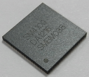
SM4109

Description

The SM4109 consists of four internal-switch regulators (main boost converter, 3.3VDD buck converter, HAVDD buck converter and 1.2VDD buck converter), two external switch regulators (VON boost converter and VOFF buck-boost converter), a negative linear regulator and a high voltage level shifting scan driver.

The main boost converter and the synchronous buck converter provide the regulated supply voltage for the panel source driver ICs. The 3.3VDD buck converter provides the supply voltage for I/O interface of the T-CON and other logic circuits.
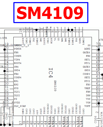
 

SM4109 datasheet pinout


Features

1. 8.7V to 14.5V Input Supply Voltage Range

2. 750kHz Switching Frequency

3 High-Efficiency Step-up Regulator
(1) Peak-current Mode Control
(2) Built-In 24V, 3.5A, 0.15Ω MOSFET

4. High-Voltage Step-down Regulator for Logic (3.3V)
(1) Peak-current Mode Control
(2) Built-In 20V, 2A, 0.25Ω MOSFET


Applications:

1. LCD TV and Monitor Panels


SM4109 Datasheet PDF

SM4109 pdf

Related articles across the web

LM32P10 Datasheet PDF – 4.7 inch LCD Module – Sharp

Part Number: LM32P10

Function: 4.7 inch, Medium Size Graphic Type LCD Module

Active area (H x V) : 96.0 x 72.0 mm

Manufacturer: Sharp

Image

LM32P10 datasheet lcd module

Description

The SHARP LM32P10 Passive Matrix Color LCD consists of 320 x 240 dots with a backlight system which uses a cold cathode fluorescent tube (CCFT).
The LCD also consists of a TSTN-type negative panel.

Features

1. Display Format : 320 x 240
2. Overall Dimensions : 148 (W) x 96 (H) x 8 max (D) mm
3. Active Area : 100 (W) x 76 (H) mm
4. Dot Pitch : 0.28 (W) x 0.28 (H) mm

Pinout
LM32P10 pinout
PIN

1 S Scan Start-Up Signal H
2 CP1 Input Data Latch Signal H ® L
3 CP2 Data Input Clock Signal H ® L
4 VDD Power Supply For Logic and LCD (+5 V) –
5 VSS Ground Potential (GND) –
6 VEE Power Supply For LCD –
7 D0 Display Data Signal H (ON), L (OFF)
8 D1 Display Data Signal H (ON), L (OFF)
9 D2 Display Data Signal H (ON), L (OFF)
10 D3 Display Data Signal H (ON), L (OFF)
11 VR1 LCD Contrast Adjust (A)
12 VR2 LCD Contrast Adjust (B)

Display Face Configuration

The LCD driver is 80 bits LSI, consisting of shift register, latch circuits, and LCD driver circuits. Display data which is externally divided into data for each row (320 dots) is sequentially transferred in the form of 4-bit parallel data through shift registers by Clock Signal CP2 from the left top of the display face.

When data of one row (320 dots) has been input, they are latched in the form of parallel data for 320 lines of signal electrodes by Latch Signal CP1. Then the corresponding drive signal is transmitted to the 320 lines of column electrodes of the LCD panel by the LCD drive circuits.

LM32P10 Datasheet


LM32P10 pdf

Other data sheets are available within the file:

Related articles across the web