W25X40 Datasheet PDF – 4M-bit, Flash Memory – Winbond

Part Number: W25X40

Function: 4M-bit, Serial Flash Memory

Package: SOP 8 pin Type

Manufactuers : Winbond

Image

W25X40

Features

1. W25X10 : 1M-bit / 128K-byte (131,072)
2. W25X20 : 2M-bit / 256K-byte (262,144)
3. W25X40 : 4M-bit / 512K-byte (524,288)
4. W25X80 : 8M-bit / 1M-byte (1,048,576)
5. 256-bytes per programmable page
6. Uniform 4K-byte Sectors / 64K-byte Blocks


Description

The W25X10 (1M-bit), W25X20 (2M-bit), W25X40 (4M-bit) and W25X80 (8M-bit) Serial Flash memories provide a storage solution for systems with limited space, pins and power. The 25X series offers flexibility and performance well beyond ordinary Serial Flash devices. They are ideal for code download applications as well as storing voice, textand data. The devices operate on a single 2.7V to 3.6V power supply with current consumption as low as 5mA active and 1µA for power-down. All devices are offered in space-saving packages.

The W25X10/20/40/80 array is organized into 512/1024/2048/4096 programmable pages of 256-bytes
each. Up to 256 bytes can be programmed at a time using the Page Program instruction.

W25X40 Datasheet

W25X40 Datasheet

Related articles across the web

95P04 Datasheet PDF – 4K (512 x 8) EEPROM, Memory

Part Number: 95P04

Function: SERIAL ACCESS SPI BUS 4K 512 x 8 EEPROM

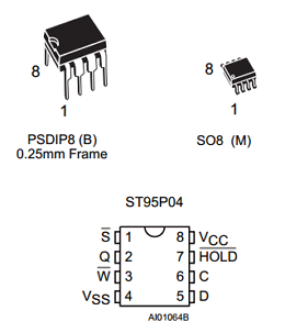
Package: DIP, SO 8 Pin Type

Manufacturer: STMicroelectronics

Image 95P04

Description

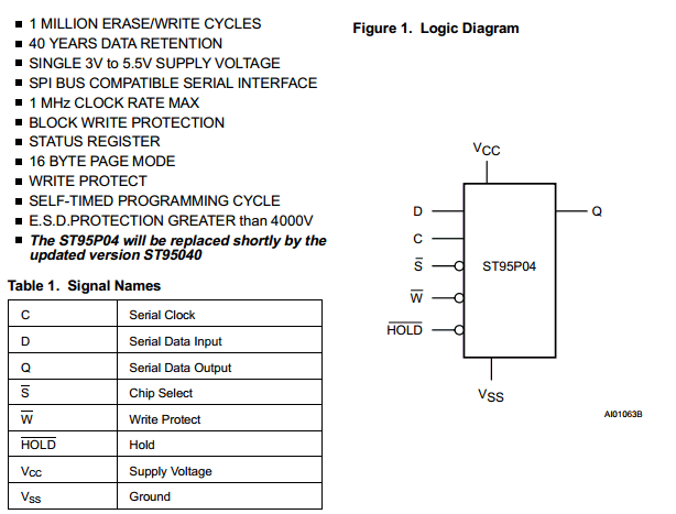
The 95P04 is a 4K bit Electrically Erasable Programmable Memory (EEPROM) fabricated with SGS-THOMSON’s High Endurance Single Polysilicon CMOS technology. The 4K bit memory is or ganised as 32 pages of 16 bytes. The memory is accessed by a simple SPI bus compatible serial interface. The bus signals are a serial clock input (C), a serial data input (D) and a serial data output (Q). The device connected to the bus is selected when the chip select input (S) goes low. Communications with the chip can be interrupted with a hold input (HOLD). The write operation is disabled by a write protect input (W).

Logic Diagram :

95P04 Datasheet

Features

1. 1 MILLION ERASE/WRITE CYCLES

2. 40 YEARS DATA RETENTION

3. SINGLE 3V to 5.5V SUPPLY VOLTAGE

4. SPI BUS COMPATIBLE SERIAL INTERFACE

5. 1 MHz CLOCK RATE MAX

6. BLOCK WRITE PROTECTION

7. STATUS REGISTER

8. 16 BYTE PAGE MODE

9. WRITE PROTECT

10. SELF-TIMED PROGRAMMING CYCLE

11. E.S.D.PROTECTION GREATER than 4000V

95P04 Datasheet PDF