A Silicon N-Channel MOS (Metal-Oxide-Semiconductor) type Field-Effect Transistor (FET) is a three-terminal semiconductor device that operates based on the field effect principle.
The Part Number is TK20A60U.
The Making information is K20A60U.
The function of this MOSFET is N-Channel, 600V, 20A, MOSFET.
The package is TO-220 Type
Manufacturer: Toshiba
Image

Description
The K20A60U is 600V, 20A, Silicon N Channel MOS Type Field Effect Transistor.
N-channel MOSFETs find widespread use in various electronic applications, such as amplifiers, switches, logic circuits, and integrated circuits (ICs).
1. Gate: The gate is composed of a metal layer separated from the channel by a thin insulating layer, typically made of silicon dioxide (SiO2). The gate voltage controls the conductivity of the channel.
2. Source: The source terminal is connected to the N-doped region of the transistor, providing a source of electrons.
3. Drain: The drain terminal is connected to the opposite end of the channel and serves as the output terminal for the current flow.
Features
• Low drain-source ON-resistance: RDS (ON) = 0.165 Ω (typ.)
• High forward transfer admittance: ⎪Yfs⎪ = 12 S (typ.)
• Low leakage current: IDSS = 100 μA (max) (VDS = 600 V)
• Enhancement-mode: Vth = 3.0 to 5.0 V (VDS = 10 V, ID = 1 mA)
[…]
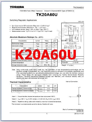
Absolute Maximum Ratings (Ta = 25°C)
1. Drain to source voltage: VDSS = 600 V
2. Gate to source voltage: VGSS = ± 30 V
3. Drain current: ID = 20 A
4. Drain power dissipation : PD = 45 W
5. Single pulse avalanche energy : Eas = 144 mJ
6. Avalanche curren : Iar = 20 A
7. Repetitive avalanche energy : Ear = 4.5 mJ
8. Channel temperature: Tch = 150 °C
9. Storage temperature: Tstg = -55 to +150 °C
Applications:
1. Switching Regulator
K20A60U PDF Datasheet


