25Q32BSIG Datasheet PDF – 32M-bit Serial Flash Memory

Part Number: 25Q32BSIG

Function: 32M-bit Serial Flash Memory

Package: SOP / DIP 8 Pin Type

Manufacturer: GigaDevice, ELM Technology

Images:

25Q32BSIG datasheet memory

Description

The GD25Q32B (32M-bit) Serial flash supports the standard Serial Peripheral Interface (SPI), and supports the Dual/Quad SPI: Serial Clock, Chip Select, Serial Data I/O0 (SI), I/O1 (SO), I/O2 (WP#), and I/O3(HOLD#). The Dual I/O data is transferred with speed of 240Mbits/s and the Quad I/O & Quad output data is transferred with speed of 480Mbits/s.

Pinout:

25Q32BSIG pinout

Features

1. Low Power Consumption
(1) 120MHz for fast read with 30PF load
(2) Dual I/O Data transfer up to 240Mbits/s
(3) Quad I/O Data transfer up to 480Mbits/s

2. High Speed Clock Frequency
(1) 20mA maximum active current
(2) 5uA maximum power down current

3. Software/Hardware Write Protection
(1) Write protect all/portion of memory via software
(2) Enable/Disable protection with WP# Pin
(3) Top or Bottom, Sector or Block selection

4. Single Power Supply Voltage
(1) Full voltage range:2.7~3.6V

Ordering Information

25Q32BSIG ordering information

Other data sheets are available within the file: GD25Q32BSIG, GD25Q32BWIG, GD25Q32BZIG, 25Q328SIG

25Q32BSIG Datasheet PDF

BQ737 pdf


Similar features and reference parts


Related articles across the web

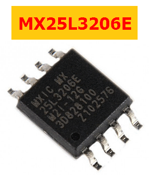
MX25L3206E Datasheet – 32M Bit CMOS Serial Flash – MXIC

Part Number: MX25L3206E

Function: 32M-BIT [x 1 / x 2] CMOS SERIAL FLASH

Manufacturer: Macronix International

Image :

MX25L3206E datasheet


Description

The MX25L3206E feature a serial peripheral interface and software protocol allowing operation on a simple 3-wire bus. The three bus signals are a clock input (SCLK), a serial data input (SI), and a serial data output (SO). Serial access to the device is enabled by CS# input. When it is in Dual Output read mode, the SI and SO pins become SIO0 and SIO1 pins for data output.


Pinout

MX25L3206E pinout
Features

1. Single Power Supply Operation
– 2.7 to 3.6 volt for read, erase, and program operations

2. Serial Peripheral Interface compatible — Mode 0 and Mode 3

3. 33,554,432 x 1 bit structure or 16,777,216 x 2 bits (Dual Output mode) structure

4. 1024 Equal Sectors with 4K byte each
– Any Sector can be erased individually

5. 64 Equal Blocks with 64K byte each
– Any Block can be erased individually

6. Program Capability
– Byte base
– Page base (256 bytes)

7. Latch-up protected to 100mA from -1V to Vcc +1V

MX25L3206E Datasheet PDF Download

25L3206E pdf


Other data sheets are available within the file: MX25L3206EMI-12G, MX25L3206EPI-12G, MX25L3206EZNI-12G

Related articles across the web