P75NF758 Datasheet – 75V, 80A, N-Ch MOSFET – ST

This is one of the types of MOSFETs and is a kind of transistor.

Part Number: P75NF758, P75NF75B, Correct PN : STP75NF75

Function: N-channel Power MOSFET ( 75V, 80A )

Package: TO-220 Type

Manufacturer: STMicroelectronics

Image

P75NF758 mosfet

Description

This is N-channel, 75V, 0.0095Ω, 80A, STripFET II Power MOSFET.

This Power MOSFET series realized with STMicroelectronics unique STripFET process has specifically been designed to minimize input capacitance and gate charge. It is therefore suitable as primary switch in advanced high efficiency, high-frequency isolated DC-DC converters for Telecom and Computer applications. It is also intended for any applications with low gate drive requirements.

Image and Pinout:
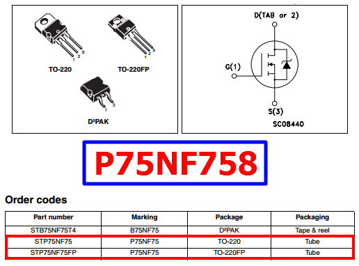
P75NF758 datasheet pinout

Absolute Maximum Ratings (Ta = 25°C)

1. Drain to source voltage: VDSS = 75 V
2. Gate to source voltage: VGSS = ± 20 V
3. Drain current: ID = 80 A
4. Channel temperature: Tch = 150 °C
5. Storage temperature: Tstg = -55 to +175 °C


Applications

1. Switching application

P75NF758 Datasheet


Related articles across the web

25P10VP Datasheet PDF – 1 Mbit Flash Memory, M25P10 – ST

Part Number: 25P10VP

Function: 1 Mbit Low Voltage Paged Flash Memory With 20 MHz Serial SPI Bus Interface

Package: SOP 8 Pin

Manufacturer: STMicroelectronics

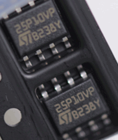
Image :

25P10VP image

Features

1. 1 Mbit PAGED Flash Memory
2. 128 BYTE PAGE PROGRAM IN 3 ms TYPICAL
3. 256 Kbit SECTOR ERASE IN 1 s TYPICAL
4. BULK ERASE IN 2 s TYPICAL
5. SINGLE 2.7 V to 3.6 V SUPPLY VOLTAGE
6. SPI BUS COMPATIBLE SERIAL INTERFACE
7. 20 MHz CLOCK RATE AVAILABLE
8. SUPPORTS POSITIVE CLOCK SPI MODES
9. DEEP POWER DOWN MODE (1 µA TYPICAL)
10. ELECTRONIC SIGNATURE
11. 10,000 ERASE/PROG CYCLES PER SECTOR
12. 20 YEARS DATA RETENTION
13. –40 TO 85°C TEMPERATURE RANGE

Pinout

25P10VP Pinout

Description

The 25P10VP ( M25P10 ) is an 1 Mbit Paged Flash Memory fabricated with STMicroelectronics High Endurance CMOS technology. The memory is accessed by a simple SPI bus compatible serial interface. The bus signals are a serial clock input (C), a serial data input (D) and a serial data output (Q).

The device connected to the bus is selected when the chip select input (S) goes low. Data is clocked in during the low to high transition of clock C, data is clocked out during the high to low transition of clock C

SIGNALS Description

Serial Output (Q)
The output pin is used to transfer data serially out of the memory. Data is shifted out on the falling edge of the serial clock.

Serial Input (D)
The input pin is used to transfer data serially into the device. It receives instructions, addresses,
and the data to be programmed. Input is latched on the rising edge of the serial clock.

Serial Clock (C)
The serial clock provides the timing of the serial interface. Instructions, addresses, or data present
at the input pin are latched on the rising edge of the clock input, while data on the Q pin changes
after the falling edge of the clock input.

Logic Diagram

25P10VP Datasheet

25P10VP Datasheet

25P10VP pdf datasheet st

Other data sheets are available within the file: M25P10-VMW6T, M25P10-AVMN6TP/X