STK412-430 Datasheet PDF – Audio Power Amplifier

Part Number: STK412-430

Function: Two-Channel Shift Power Supply Audio Power Amplifier ICs 150W + 150 W

Package: SIP 18 Pin Type

Manufacturer: SANYO (Panasonic)

Image :

STK412-430 image

Description

The STK412-430 series are class H audio power amplifier hybrid ICs that feature a built-in shift power  upply circuit. These Provide ICs high efficiency audio power amplification by controlling (switching) the supply voltage supplied to the power transistors according to the detected level of the input audio signal.

1. Pin compatible IC series that covers power ratings from 50 W × 2 channels to 180 W × 2 channels at 0.7 or 0.8% THD, 20 Hz to 20 kHz. This allows the use of a common PCB for all output classes.

2.  The pin arrangement is also unified with that of the three-channel STK413-000 series. This means that PCBs designed for three-channel models can also be used for two-channel models.

Reference Circuit : STK412-410
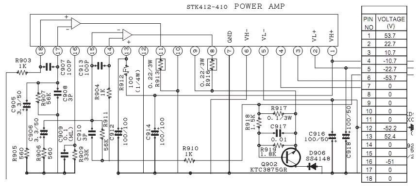
STK412-410 datasheet, pinout

Features

  • Class H amplification with dynamic supply voltage switching
  • High output power capability for stereo applications
  • Low total harmonic distortion for clean audio output
  • Low noise with high signal-to-noise ratio
  • Built-in thermal protection circuitry
  • Short-circuit and overload protection
  • Compact 18-pin SIP package for easy mounting

Typical Circuit Usage

  • Stereo power amplifier stages in hi-fi systems
  • Audio output stages in home theater receivers
  • High-power speaker driving circuits
  • Integrated amplifier designs for consumer electronics
  • Custom audio amplifier modules

How to Choose This Part

  • Choose for high-output stereo applications requiring efficient Class H topology
  • Suitable when compact hybrid modules simplify amplifier design
  • Ideal for designs needing integrated protection features
  • Consider thermal constraints and required output power levels
  • Verify compatibility with existing power supply architecture

Applications

  • Hi-Fi audio amplifiers
  • Home theater systems
  • High-power stereo systems
  • Professional audio equipment
  • Multimedia speaker systems

Alternative / Equivalent Products

  • STK412-410
  • STK412-440
  • STK404-130S
  • LM3886
  • TDA7294

Other data sheets are available within the file: STK350-000, STK350-010, STK350-020, STK350-030, STK350-040

STK412-430 Datasheet

STK412-430 pdf
STK412-430

STK412-150 Datasheet

STK412-430 pdf

4558D Datasheet, JRC NJM4558D PDF – Dual OP AMP

The 4558D (also known as NJM4558D / JRC4558) is a dual operational amplifier consisting of two internally compensated, high-gain op-amps integrated on a single silicon die.

Part Number: JRC4558, NJM4558D

Function: DUAL OPERATIONAL AMPLIFIER

Package: DIP 8 Pin Type

Manufacturer: Japan Radio Corporation

Image

4558D datasheet pdf

Description

The 4558D, NJM4559 integrated circuit is a dual high-gain operational amplifier internally compensated and constructed on a single silicon chip using an advanced epitaxial process.

Combining the features of the NJM741 with the close parameter matching and tracking of a dual device on a monolithic chip results in unique performance characteristics. Excellent channel separation allows the use of the dual device in single NJM741 operational amplifier applications providing density. It is especially well suited for applications in differential-in, differential-out as well as in potentiometric amplifiers and where gain and phase matched channels are mandatory.

Features

  • Wide operating supply range: ±4V to ±18V
  • High open-loop voltage gain (~100 dB typical)
  • High input resistance (~5 MΩ typical)
  • Good channel separation and matching
  • Bipolar input stage (better noise than early general-purpose op-amps)
  • Stable without external compensation
  • Available in standard DIP and SOP packages

Pin Configuration (8-Pin Dual Op-Amp)

4558d datasheet

  • Pin 1: Output 1
  • Pin 2: Inverting Input 1 (-)
  • Pin 3: Non-inverting Input 1 (+)
  • Pin 4: V– (Negative supply or GND)
  • Pin 5: Non-inverting Input 2 (+)
  • Pin 6: Inverting Input 2 (-)
  • Pin 7: Output 2
  • Pin 8: V+ (Positive supply)

Key Electrical Characteristics (Typical)

  • Open-loop gain: ~100 dB
  • Input bias current: ~200 nA
  • Input offset voltage: ~1–5 mV
  • Slew rate: ~1 V/µs
  • Gain-bandwidth product: ~3 MHz

Typical Circuit Usage

  • Audio preamplifiers and tone control circuits
  • Active filters (low-pass, high-pass, band-pass)
  • Signal conditioning and buffering
  • Differential amplifier stages
  • Integrator and comparator (non-critical timing)

How to Choose This Part

  • Use when moderate performance and low cost are priorities
  • Ideal for audio-frequency applications (<100kHz)
  • Suitable when dual op-amp matching is required
  • Not recommended for precision low-offset or rail-to-rail designs
  • Consider modern CMOS op-amps for low-power or high-speed needs

Applications

  • Audio amplifiers and mixers
  • Instrumentation and signal processing
  • Industrial analog control circuits
  • Consumer electronics
  • General-purpose analog design

Alternative / Equivalent Products

  • LM358 (single-supply, lower power alternative)
  • TL072 (JFET input, lower noise for audio)
  • NE5532 (high-performance audio op-amp)
  • OPA2134 (audiophile-grade op-amp)
  • MC1458 (older equivalent dual op-amp)

Other data sheets are available within the file: JRC4558, JRC4559, NJM4558M, NJM4558L, NJM4558V

4558D Datasheet PDF Download

JRC4558 pdf