G4PC40W PDF – IRG4PC40W ( 600V, IGBT, TO-247AC )

Part Number: G4PC40W, IRG4PC40W

Function: 600V, 40A, IGBT ( The IGBT is insulated-gate bipolar transistor. )

Package: TO-247AC type

Manufacturer: IRFG4PC40W pdf pinout

Description

THE G4PC40W IS INSULATED GATE BIPOLAR TRANSISTOR. IGBT stands for Insulated-Gate Bipolar Transistor. It is a type of power semiconductor device that combines the advantages of bipolar transistors (high voltage and current handling capability) and field-effect transistors (fast switching and low on-state resistance).

They are also used in applications where high voltage and high current are required, such as in welding equipment and induction heating.

An IGBT consists of a P-N-P-N structure with an insulated gate, which is used to control the flow of current between the emitter and collector terminals. When a positive voltage is applied to the gate terminal, it creates a conducting channel between the emitter and collector, allowing current to flow.

Features:

• Designed expressly for Switch-Mode Power Supply and PFC (power factor correction) applications

• Industry-benchmark switching losses improve efficiency of all power supply topologies

• 50% reduction of Eoff parameter

• Low IGBT conduction losses

• Latest-generation IGBT design and construction offers tighter parameters distribution, exceptional reliability VCES = 600V G E VCE(on) typ. = 2.05V @VGE = 15V, IC = 20A n-channel


G4PC40W datasheet igbt


Benefits:

• Lower switching losses allow more cost-effective operation than power MOSFETs up to 150 kHz (“hard switched” mode)

• Of particular benefit to single-ended converters and boost PFC topologies 150W and higher

• Low conduction losses and minimal minority-carrier recombination make these an excellent option for resonant mode switching as well (up to >>300 kHz) TO-247AC


Absolute Maximum Ratings (Tc = 25°C)

1. Collector-to-Emitter Breakdown Voltage : Vces = 600 V

2. Continuous Collector Current : 40 A

3. Pulsed Collector Current: Icm = 160 A

4. Maximum Power Dissipation : PD = 160 W

5. Channel temperature: Tch = 150 °C

6. Storage temperature: Tstg = -55 to +150 °C


G4PC40W PDF Datasheet

RJP63F3DPP-M0 PDF Datasheet – 630V, N-Ch, IGBT

Part Number: RJP63F3DPP-M0

Function: 630V, 40A, N-Channel IGBT

Package: TO-220FL Type

Manufacturer: Renesas

Images:RJP63F3DPP-M0 pdf pinout

Description

RJP63F3DPP-M0 is 630V, Silicon N Channel IGBT.

IGBT stands for Insulated-Gate Bipolar Transistor. It is a type of power semiconductor device that combines the advantages of bipolar transistors (high voltage and current handling capability) and field-effect transistors (fast switching and low on-state resistance).

They are also used in applications where high voltage and high current are required, such as in welding equipment and induction heating.

An IGBT consists of a P-N-P-N structure with an insulated gate, which is used to control the flow of current between the emitter and collector terminals. When a positive voltage is applied to the gate terminal, it creates a conducting channel between the emitter and collector, allowing current to flow.

When the gate voltage is removed, the channel is turned off, and the IGBT becomes an open switch.

These advantages include high voltage and current handling capability, fast switching speed, low switching losses, and low on-state resistance.

Applications:

1. High Speed Power Switching

Features

1. Trench gate and thin wafer technology (G6H series)

2. Low collector to emitter saturation voltage VCE(sat) = 1.7 V typ

3. High speed switching tf = 100 ns typ

4. Low leak current ICES = 1 μA max

5. Isolated package TO-220FL

Package code :

PRSS0003AF-A) (Package name: TO-220FL) C G 1. Gate 2. Collector 3. Emitter

RJP63F3DPP-M0 datasheet igbt

Absolute Maximum Ratings (Ta = 25°C) :

1. Collector to Emitter Voltage: Vces = 630 V

2. Gate to Emitter Voltage: VGes = ± 30 V

3. Collector Current: Ic = 40 A

4. Collector dissipation: Pc = 30 W

5. Operating Junction Temperature: Tch = -55 to +150 °C

6. Storage temperature: Tstg = -55 to +150 °C

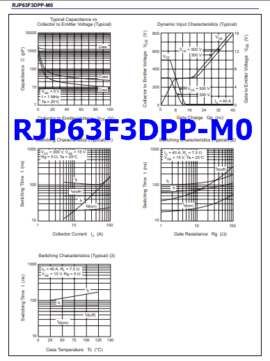
Notes: 3. Pulse test. R07DS0321EJ0200 Rev.2.00 May 26, 2011 Page 2 of 6 RJP63F3DPP-M0 Preliminary Main Characteristics Maximum Safe Operation Area 1000 100 10 PW Typical Output Characteristics (1) Pulse Test Ta 4 6 8 10 Collector to Emitter Voltage VCE (V) Gate to Emitter Voltage VGE (V) Collector to Emitter Saturation Voltage vs. Gate to Emitter Voltage (Typical) Collector […]


RJP63F3DPP-M0 PDF Datasheet