TC58TEG6DDKTA00 Datasheet – NAND Memory Toggle DDR1.0

Part Number: TC58TEG6DDKTA00

Function: NAND Memory Toggle DDR1.0

Package: TSOP48 Pin

Manufacturer: Toshiba

Image
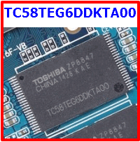
TC58TEG6DDKTA00 NAND memory Toggle DDR

Description

Toggle DDR, TC58TEG6DDKTA00 is a NAND interface for high performance applications which support data read and write operations using bidirectional DQS. Toggle DDR NAND has implemented ’Double Data Rate’ without a clock. It is compatible with functions and command which have been supported in conventional type NAND(i.e. SDR NAND) while providing high data transfer rate based on the high-speed Toggle DDR Interface and saving power with separated DQ voltage. For applications that require high capacity and high performance NAND, Toggle DDR NAND is the most appropriate.

NAND memory is a type of non-volatile flash memory that is commonly used for data storage in electronic devices such as smartphones, tablets, and solid-state drives (SSDs). The term “NAND” stands for “NOT AND,” which refers to the basic logic gate used in the memory’s construction.


Features
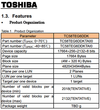
TC58TEG6DDKTA00 features

Toggle DDR1.0 NAND supports the interface speed of up to 100 MHz, which is faster than the data transfer rate offered by SDR NAND. Toggle DDR NAND transfers data at high speed using DQS signal that behaves as a clock, and DQS shall be used only when data is transferred for optimal power consumption.

This device supports both SDR interface and Toggle DDR interface. When starting, the device is activated in SDR mode. The interface mode can be changed into Toggle DDR interface utilizing specific command issued by the Host.

Pinout
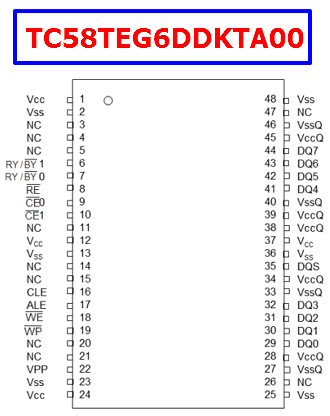
TC58TEG6DDKTA00 datasheet pinout

TC58TEG6DDKTA00 Datasheet PDF


Related articles across the web

25L3206E Datasheet – 32M Bit CMOS Serial Flash – MXIC

Part Number: 25L3206E

Function: 32M-BIT [x 1 / x 2] CMOS SERIAL FLASH

Package: SOP 8 Pin, SOP 16 Pin, 24-Ball BGA Type

Manufacturer: Macronix International

Image:

25L3206E datasheet


Description

The 25L3206E feature a serial peripheral interface and software protocol allowing operation on a simple 3-wire bus. The three bus signals are a clock input (SCLK), a serial data input (SI), and a serial data output (SO). Serial access to the device is enabled by CS# input. When it is in Dual Output read mode, the SI and SO pins become SIO0 and SIO1 pins for data output.

After program/erase command is issued, auto program/ erase algorithms which program/ erase and verify the specified page or sector/block locations will be executed. Program command is executed on byte basis, or page basis, or word basis for erase command is executes on sector, or block, or whole chip basis.


Pinout

25L3206E pinout

Features

1. Single Power Supply Operation
– 2.7 to 3.6 volt for read, erase, and program operations

2. Serial Peripheral Interface compatible — Mode 0 and Mode 3

3. 33,554,432 x 1 bit structure or 16,777,216 x 2 bits (Dual Output mode) structure

4. 1024 Equal Sectors with 4K byte each
– Any Sector can be erased individually

5. 64 Equal Blocks with 64K byte each
– Any Block can be erased individually

6. Program Capability
– Byte base
– Page base (256 bytes)

7. Latch-up protected to 100mA from -1V to Vcc +1V


PERFORMANCE :

1. High Performance
– Fast access time: 86MHz serial clock
– Serial clock of Dual Output mode : 80MHz
– Fast program time: 1.4ms(typ.) and 5ms(max.)/page
– Byte program time: 9us (typical)


Other data sheets are available within the file:

25L3206EMI-12G, 25L3206EPI-12G, 25L3206EZNI-12G

25L3206E Datasheet PDF Download

25L3206E pdf


Related articles across the web