11N06LT PDF – 55V, 11A, MOSFET – PHB11N06LT

Part Number: 11N06LT, PHB11N06LT

Function: 55V, 11A, MOSFET

Package: SOT-428, SOT404 Type

Manufacturer: NXP Semiconductor, Philips Semiconductor

Images:PHB11N06LT pdf mosfet
Description

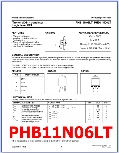
This is N-channel enhancement mode, logic level, field-effect power transistor in a plastic envelope using ’trench’ technology. The device has very low on-state resistance. It is intended for use in dc to dc converters and general purpose switching applications. The PHB11N06LT is supplied in the SOT404 surface mounting package. The PHD11N06LT is supplied in the SOT428 surface mounting package.

A Trench MOS transistor is a type of metal-oxide-semiconductor (MOS) transistor that is constructed using a trench isolation structure. This design allows for better control of the electric field and reduced parasitic effects, making it a popular choice for power devices and high-voltage applications.

Trench MOS transistors find extensive use in power electronics, including motor control, power supplies, automotive applications, and high-voltage converters. They are employed in various devices such as power MOSFETs, insulated-gate bipolar transistors (IGBTs), and trench gate field-effect transistors (TGFETs).


Features:

• ’Trench’ technology

• Very low on-state resistance

• Fast switching

• Stable off-state characteristics

• High thermal cycling performance

• Low thermal resistance
 

PHB11N06LT datasheet pinout

11N06LT PDF Datasheet

IRF142 PDF Datasheet – 100V, N-Ch, MOSFET, Transistor

Part Number: IRF142

Function: 100V, 24A, N-Channel MOSFET Transistor

Package: TO-3 Type

Manufacturer: Inchange Semiconductor

Images:IRF142 pdf pinout

Description

IRF142 is 100V, 24A, N-Channel MOSFET (INCHANGE Semiconductor).

Features

1. Drain Current ID=24A@ TC=25℃

2. Drain Source Voltage- : VDSS= 100V(Min)

3. Static Drain-Source On-Resistance : RDS(on) =0.11Ω(Max)

4. High Power,High Speed Applications


Absolute Maximum Ratings (Ta = 25°C)

1. Drain to source voltage: VDSS = 100 V

2. Gate to source voltage: VGSS = ± 20 V

3. Drain current: ID = 24 A

4. Total Power Dissipation: Pd = 125 W

5. Channel temperature: Tch = 150 °C

6. Storage temperature: Tstg = -55 to +150 °C

IRF142 datasheet mosfet


Applications:

1. Switching power supplies

ELECTRICAL CHARACTERISTICS (TC=25℃) :

SYMBOL PARAMETER CONDITIONS V(BR)DSS Drain-Source Breakdown Voltage VGS=0; ID=250µA VGS(TH) Gate Threshold Voltage VDS= VGS; ID=250µA RDS(ON) Drain-Source On-stage Resistance VGS=10V; ID=8A IGSS Gate Source Leakage Current VGS=±20V;VDS=0 IDSS Zero Gate Voltage Drain Current VDS=100V; VGS=0 VSD Diode Forward Voltage IS=24A; VGS=0 Ciss Input Capacitance Crss Reverse Transfer Capacitance Coss Output Capacitance VDS=25V; VGS=0V; fT=1MHz tr Rise Time td(on) Turn-on Delay Time tf Fall Time ID=15A; VDD=50V; RL=4.7Ω td(off) Turn-off Delay Time isc Product Specification.  […]


IRF142 PDF Datasheet

IRF142 pdf