This post explains for the nand Flash memory H27UCG8T2ATR-BC.
The Part Number is H27UCG8T2ATR-BC. The package is TSOP-48/SDP.
The function of this semiconductor is 64Gb(8192M x 8bit) Legacy MLC NAND Flash.
Manufacturer: Hynix
Preview images :

Description
The product part NO. H27UCG8T2ATR-BC is a single 3.3V 64Gbit NAND flash memory. The Device contains 2 planes in a single die. Each plane is made up of the 2090 blocks. Each block consists of 256 programmable pages. Each page contains 8,832bytes. The pages are subdivided into an 8,192byte main data storage area with a spare 640byte district. Page program operation can be performed in typical 1500us, and a single block can be erased in typical 5ms […]
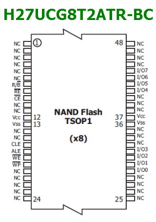
Pinout

Feature
1. Power Supply Voltage
– VCC / VCCq= 2.7V ~ 3.6V
2. Organization
– Page Size : 8192 + 640(Spare) bytes
– Block Size : 2M + 160K bytes, 256pages
– Plane Size : 2048 + 42(Extended) blocks
– Device Size : 4096 + 84(Extended) blocks
3. Page Read Time
– Random Read Time (tR) : 60/80us(Typ./Max)
– Sequential Access (tRC/tWC) : 16ns(Min.)
4. Page Write Time
– Page Program Time : 1500(Typ.)
5. Block Erase Time
– Block Erase Time : 5.0ms(Typ.)
Bad Block Management
Devices with Bad Blocks have the same quality level and the same AC and DC characteristics as devices where all the blocks are valid. A Bad Block does not affect the performance of valid blocks because it is isolated from the bit line and common source line by a select transistor. The devices are supplied with all the locations inside valid blocks erased (FFh). The Bad Block Information is written prior to shipping. Any block where the 1st Byte in the spare area of the First and Last page does not contain FFh is a Bad Block. The Bad Block Information must be read before any erase is attempted as the Bad Block Information may be erased.
H27UCG8T2ATR-BC Datasheet