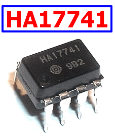
NAND01GW3B Datasheet – 1 Gbit, NAND Flash Memory – ST

Part Number: NAND01GW3B

Function: 1 Gbit, 1.8V/3V, NAND Flash Memory

Package: TSOP48, VFBGA63 type

Manufacturer: STMicroelectronics ( st.com )

Image

NAND01GW3B Nand Flash Memory

Description

The NAND01GW3B is 1 Gbit, NAND Flash Memory.

The NAND Flash 2112 Byte/ 1056 Word Page is a family of non-volatile Flash memories that uses NAND cell technology. The devices range from 1 Gbit to 8 Gbits and operate with either a 1.8V or 3V voltage supply. The size of a Page is either 2112 Bytes (2048 + 64 spare) or 1056 Words (1024 + 32 spare) depending on whether the device has a x8 or x16 bus width.

What is NAND Flash Memory?

NAND flash memory is named after the Boolean logic function “NOT-AND” (NAND), which describes its internal circuit design.

NAND flash memory is organized as a series of memory cells, each of which is composed of a floating-gate transistor and a control gate transistor. The state of each memory cell is determined by the amount of electrical charge stored on the floating gate.

One of the key advantages of NAND flash memory is its high storage density, which allows for large amounts of data to be stored in a small physical space. It also has a fast read speed and low power consumption, making it well-suited for use in portable devices.

Product List:
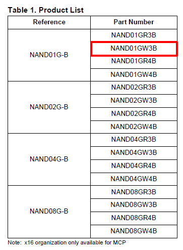
NAND01GW3B datasheet

The address lines are multiplexed with the Data Input/Output signals on a multiplexed x8 or x16 Input/Output bus. This interface reduces the pin count and makes it possible to migrate to other densities without changing the footprint.

Pinout
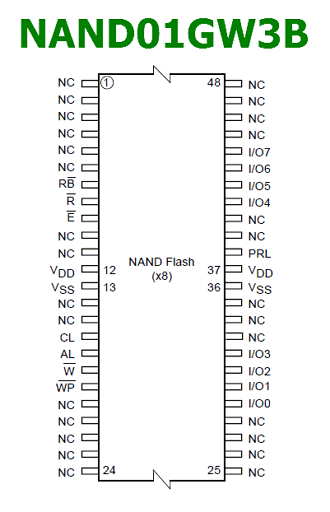
NAND01GW3B pinout

Features

1. HIGH DENSITY NAND FLASH MEMORIES
(1) Up to 8 Gbit memory array
(2) Up to 64Mbit spare area
(3) Cost effective solutions for mass storage applications

2. NAND INTERFACE
(1) x8 or x16 bus width
(2) Multiplexed Address/ Data
(3) Pinout compatibility for all densities

Other data sheets are available within the file: NAND01GR3B, NAND01GR4B, NAND01GW4B

NAND01GW3B Datasheet PDF Download

NAND01GW3B pdf


Related articles across the web

M312L2828ET0 Datasheet – DDR SDRAM – Samsung ( PDF )

Part Number: M312L2828ET0

Function : DDR SDRAM Registered Module, 1GB, 128M x 72 ECC Module

Manufacturer: Samsung

Image M312L2828ET0 image

Features

• VDD : 2.5V ± 0.2V, VDDQ : 2.5V ± 0.2V for DDR266, 333
• VDD : 2.6V ± 0.1V, VDDQ : 2.6V ± 0.1V for DDR400
• Double-data-rate architecture; two data transfers per clock cycle
• Bidirectional data strobe [DQ](x4,x8) & [L(U)DQS] (x16)
• Differential clock inputs(CK and CK)
• DLL aligns DQ and DQS transition with CK transition
• Programmable Read latency : DDR266(2, 2.5 Clock), DDR333(2.5 Clock), DDR400(3 Clo
• Programmable Burst length (2, 4, 8)
• Programmable Burst type (sequential & interleave)
• Edge aligned data output, center aligned data input
• Auto & Self refresh, 7.8us refresh interval(8K/64ms refresh)
• Serial presence detect with EEPROM
• SSTL_2 Interface
• 66pin TSOP II and 60 ball FBGA Leaded & Pb-Free(RoHS compliant) package

Block Diagram

M312L2828ET0 datasheet

Description

DRAM is a type of RAM (random access memory) used as the main memory in several computing devices, such as desktop and notebook computers, servers, and high-end workstations. It is the most widely used semiconductor memory used in current generation computers, and offers several significant advantages, such as structural simplicity, very high packing densities (number of bytes that can be stored per unit of chip area), low power consumption, and sufficiently high data read/write speeds. Several types of DRAM are presently available for deployment on various computing platforms, such as home/personal computers, portable computers, and network servers. This type of memory has undergone several innovative technological developments and offers very high price/performance ratios.

Official Homepage: https://semiconductor.samsung.com/

M312L2828ET0 Datasheet