K2529 Datasheet PDF – N-Ch, 60V, 50A, MOSFET, Transistor

Part Number: K2529

Function: 60V, 50A, N-Channel MOSFET

Package: TO-220CFM type

Manufacturer: Renesas Electronics

Image and Pinouts:
K2529 datasheet

Description

This is a 60V, 50A, Silicon N Channel MOSFET.

The K2529 is a N-channel power MOSFET (Metal-Oxide-Semiconductor Field-Effect Transistor) manufactured by Renesas Electronics. It is commonly used as a switch in power electronics applications, where its low on-resistance and fast switching speed make it well-suited for high-efficiency power conversion systems.

The 2SK2529 has a maximum drain-source voltage of 600V and a maximum drain current of 20A,
making it suitable for high voltage, high current applications.
Its small form factor and high power density make it a popular choice for compact power supplies,
motor drives, and other power conversion systems.

Features

1. Low on-resistance

2. RDS(on)= 7 mΩtyp.

3. High speed switching

4. 4 V gate drive device can be driven from 5 V source

components

Absolute Maximum Ratings (Ta = 25°C)

1. Drain to source voltage: VDSS = 60 V

2. Gate to source voltage: VGSS = ± 20 V

3. Drain current: ID = 50 A

4. Channel dissipation: Pch = 35 W

5. Channel temperature: Tch = 150 °C

6. Storage temperature: Tstg = -55 to +150 °C


Application:

1. High speed power switching


K2529 Datasheet PDF Download


K2529 pdf

Other data sheets are available within the file: 2SK2529
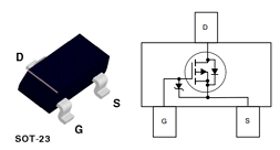
FDV302P Datasheet PDF – 25V, 0.12A, P-Ch, MOSFET

Part Number: FDV302P

Function: – 25V, – 0.12A, Digital FET, P-Channel, Transistor

Package: SOT-23 Type

Manufacturer: Fairchild Semiconductor

Image and Pinouts:

FDV302P datasheet


Description

This P-Channel logic level enhancement mode field effect transistor is produced using Fairchild’s proprietary, high cell density, DMOS technology. This very high density process is especially tailored to minimize on-state resistance. This device has been designed especially for low voltage
applications as a replacement for digital transistors. Since bias resistors are not required, this one P-channel FET can replace several digital transistors with different bias resistors such as the DTCx and DCDx series.

Features

1. Very low level gate drive requirements allowing direct operation in 3V circuits. VGS(th) < 1.5V.

2. Gate-Source Zener for ESD ruggedness. >6kV Human Body Model

3. Compact industry standard SOT-23 surface mount package.

4. Replace many PNP digital transistors (DTCx and DCDx) with one DMOS FET.


Absolute Maximum Ratings (Ta = 25°C)

1. Drain to source voltage: VDSS = – 25 V

2. Gate to source voltage: VGSS = ± 8 V

3. Drain current: ID = – 0.12 A

4. Maximum Power Dissipation: Pd = 0.35 W

5. Channel temperature: Tch = 150 °C

6. Storage temperature: Tstg = -55 to +150 °C

Other data sheets are available within the file: FDV302


FDV302P Datasheet PDF Download


FDV302P pdf