BC337 Datasheet – 45V, 0.8A, NPN Amplifier Transistor

What is BC337?

It is a popular general-purpose NPN transistor commonly used in electronic circuits for amplification and switching purposes. It has a maximum current rating of 0.8 A and a maximum voltage rating of 45 V. The transistor has a high current gain, making it suitable for low-level signal amplification. The BC337 is housed in a TO-92 package, which makes it easy to use in various electronic projects.

Part Number: BC337

Function: 45V, 0.8A, NPN Silicon Amplifier Transistor

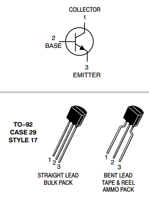
Package: TO-92 Type

Manufacturer: ON Semiconductor

Pinout BC337 Pinout

Advantages Vs Disadvantages

Advantages:

1. It is a low-cost transistor that is widely available and easy to use in various electronic projects.

2. The transistor has a high current gain, which makes it suitable for low-level signal amplification and other applications where high gain is needed.

3. The TO-92 package makes the BC337 easy to use in various electronic circuits.

Disadvantages:

1. The maximum voltage rating of 45 V may not be sufficient for some high-voltage applications.

2. The maximum current rating of 800 mA may not be sufficient for some high-current applications.

3. The BC337 is a bipolar junction transistor (BJT) and may not be suitable for some high-frequency applications that require a field-effect transistor (FET).

BC337 Datasheet PDF

BC337 Datasheet PDF Onsemi

Part numbers of commonly used NPN transistors

(1) BC547 – NPN general-purpose transistor ( 45V, 100mA )
(2) BC337 – NPN general-purpose transistor
(3) 2N2222 – NPN switching transistor ( 40V, 0.5A )
(4) 2N3904 – NPN general-purpose transistor
(5) PN2222 – NPN small signal transistor
(6) MPSA42 – NPN high-voltage transistor for switching and amplifier applications
(7) TIP120 – NPN Darlington transistor for high current applications

FAQs:

Q: What is the main difference between an NPN and PNP transistor?
A: The main difference between an NPN and PNP transistor is the direction of current flow in their base, emitter, and collector regions.

Q: Which type of transistor is more commonly used?
A: NPN transistors are more commonly used because they are easier to manufacture and have better performance characteristics than PNP transistors.

Q: What are some applications of NPN and PNP transistors?
A: NPN and PNP transistors are used in a wide range of electronic devices, including amplifiers, switches, oscillators, and voltage regulators.

Datasheet Download : https://www.onsemi.com/pub_link/Collateral/BC337-D.PDF


Related articles across the web

1803DFH Transistor – NPN, 1500V, TO-220FH (ST1803DFH)

Part Number: 1803DFH, ST1803DFH

Function: 1500V, 10A, NPN Transistor

Package: TO-220FH Type

Manufacturer: ST Microelectronics

Images:

1803DFH Transistor pdf

Description

The 1803DFH is NPN Power Transistor.

Applications:
HIGH VOLTAGE FAST-SWITCHING NPN POWER TRANSISTOR

NEW Fully Plastic TO-220 for HIGH VOLTAGE Applications s NEW SERIES, ENHANCED PERFORMANCE s INTEGRATED FREE WHEELING DIODE s HIGH VOLTAGE CAPABILITY ( > 1500 V ) s HIGH SWITCHING SPEED s TIGTHER hfe CONTROL s IMPROVED RUGGEDNESS s FULLY INSULATED PACKAGE (U.L. COMPLIANT) FOR EASY MOUNTING s CREEPAGE DISTANCE PATH > 4 mm s Applications: s HORIZONTAL DEFLECTION FOR COLOR TVS Description The device is manufactured using Diffused Collector technology for more stable operation Vs base drive circuit variations resulting in very low worst case dissipation. TO-220FH INTERNAL SCHEMATIC DIAGRAM RBE =20 Ω Typ.

ABSOLUTE MAXIMUM RATINGS Symbol V CBO V CEO V EBO IC I CM IB P tot V isol T stg Tj Parameter Collector-Base Voltage (I E = 0) Collector-Emitter Voltage (I B = 0) Emitter-Base Voltage (I C = 0) Collector Current Collector Peak Current (t p < 5 ms) Base Current Total Dissipation at T c = 25 o C Insulation Withstand Voltage (RMS) from All Three Leads to External Heatsink Storage Temperature Max. Operating Junction Temperature Value 1500 600 7 10 15 4 40 2500 -65 to 150 150 Unit V V V A A A W V o o C C December 2002 1/6 ST1803DFH THERMAL DATA R thj-case Thermal Resistance Junction-case Max 3.125 o C/W ELECTRICAL CHARACTERISTICS (Tcase = 25 oC unless otherwise specified) Symbol I CES I EBO Parameter Collector Cut-off Current (V BE = 0) Emitter Cut-off Current (I C = 0) Emitter-Base Breakdown Voltage (I C = 0) Collector-Emitter Saturation Voltage Base-Emitter Saturation Voltage DC Current Gain  ts tf Diode Forward Voltage INDUCTIVE LOAD Storage Time Fall Time ∗ Pulsed: Pulse duration = 300 µs, duty cycle 1.5 % Safe Operating Area Thermal Impedance 2/6 ST1803DFH Derating Curve Output Characteristics Collector Emitter Saturation Voltage Base Emitter Saturation Voltage DC Current Gain DC Current Gain 3/6 ST1803DFH Power losses Switching Time Inductive Load Reverse Biased SOA Figure 1: Inductive Load Switching Test Circuit.  […]

1803DFH pinout datasheet

1803DFH PDF Datasheet