25Q64FV PDF Datasheet – W25Q64FV, 64M-Bit Flash Memory

This post explains for the semiconductor 25Q64FV, W25Q64FV.

The Part Number is 25Q64FV.

The function of this semiconductor is 64M-Bit Serial Flash Memory.

Manufacturer: Winbond

Image
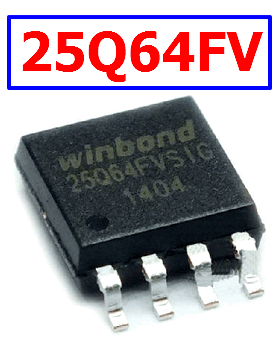
25Q64FV datasheet memory

Description

The 25Q64FV (64M-bit) Serial Flash memory provides a storage solution for systems with limited space, pins and power. The 25Q series offers flexibility and performance well beyond ordinary Serial Flash devices. They are ideal for code shadowing to RAM, executing code directly from Dual/Quad SPI (XIP) and storing voice, text and data. The device operates on a single 2.7V to 3.6V power supply with current consumption as low as 4mA active and 1µA for power-down. All devices are offered in space-saving packages.

Pinout

components

Features

Highest Performance Serial Flash

1. 104MHz Standard/Dual/Quad SPI clocks
2. 208/416MHz equivalent Dual/Quad SPI
3. 50MB/S continuous data transfer rate
4. More than 100,000 erase/program cycles
5. More than 20-year data retention

25Q64FV Datasheet

Posts related to ‘ Memory ‘

Part number Description
AM29F800BB-55EE 8 Mbit, Erase Flash Memory
H9TQ17ABJTMC 16GB, NAND Flash Memory
K5L5563CAA-D770 256Mbit NOR Flash Memory
W25Q32 32M-bit Serial Flash Memory – Winbond
PM25LD010 1 Mbit Serial Flash Memory
25Q64 64M-Bit Serial Flash Memory – Winbond
KLM8G1WEMB-B031 8GB eMMC, NAND Flash Memory
H27U2G8F2CTR 2 Gbit (256M x 8 bit) NAND Flash Memory
AM29F016B 16 Megabit, Flash Memory
25032BVSIG Serial Flash Memory – Winbond


SN65LVDS311 Datasheet PDF – 27 Bit Display Transmitter

Part Number: SN65LVDS311

Function: Programmable 27 Bit Display Serial Interface Transmitter

Package: DSBGA 49 Pin Type

Manufacturer: Texas Instruments

Image

SN65LVDS311 datasheet pdf


Description

The SN65LVDS311 serializer transmits 27 parallel input data over 1, 2, or 3 serial output links. The device pinout is optimized to interface with the OMAP3630 application processor. The device loads a shift register with the 24 pixel bits and 3 control bits
from the parallel CMOS input interface. The data are latched into the device by the pixel clock, PCLK. In addition to the 27 bits, the device adds a parity bit and two reserved bits for a total number of 30 serial bits. The parity bit allows a receiver to detect single
bit errors. Odd parity is implemented. The serial shift register is uploaded through 1, 2, or 3 serial outputs at 30, 15, or 10 times the pixel clock data rate. A copy of the pixel clock is output on an additional differential output. The serial data and clock are transmitted via Sub Low-Voltage Differential Signaling (SubLVDS) lines. The SN65LVDS311 supports three power modes (Shutdown, Standby and Active) to conserve power.

Pinouts:

SN65LVDS311 pinout

Features

1. 2.8 × 2.8mm package size
2. 1.8V input signal swing
3. 24-Bit RGB Data, 3 Control Bits, 1 Parity Bit and 2 Reserved Bits Transmitted over 1, 2 or 3 Differential Lines
4. SubLVDS Differential Voltage Levels
5. Three Operating Modes to Conserve Power
(1) Active-Mode QVGA 17.4mW (typ)
(2) Active-Mode VGA 28.8mW (typ)
(3) Shutdown Mode ≈ 0.5μA (typ)
(4) Standby Mode ≈ 0.5μA (typ)
6. ESD Rating > 3kV (HBM)
7. Pixel Clock Range of 4MHz–65MHz
8. Failsafe on all CMOS Inputs
9. Typical Application: Cameras, Embedded Computers

Official Homepage: https://www.ti.com/product/SN65LVDS311

Other data sheets are available within the file: SN65LVDS311YFFR, SN65LVDS311YFFT

SN65LVDS311 Datasheet PDF Download


SN65LVDS311 pdf