MRF455 Datasheet PDF – 18V, 15A, RF Power NPN Transistor

Part Number: MRF455

Function: The RF Line NPN Silicon Power Transistor 60W, 30MHz, 12.5V

Package: CASE 211-07, STYLE1

Manufacturer: Motorola Semiconductor, MACOM

Image
MRF455 datasheet

Description

Thise deive designed for power amplifier applications in industrial, commercial and amateur radio equipment to 30 MHz.

•  Specified 12.5 V, 30 MHz characteristics

(1) Output power = 60 W

(2) Minimum gain = 13 dB

(3)  Efficiency = 55%

Absolute maximum ratings ( Ta=25°C )

1. Collector to Emitter Voltage: Vceo = 18 V
2. Collector to Emitter Voltage : Vces = 36 V
3. Emitter to Base Voltage: Vebo = 4 V
4. Collector Current: Ic = 15 A
5. Total Device Dissipation: Pd = 175 W
6. Junction Temperature: Tj = 150°C
7. Storage Temperature: Tsg = -65 ~ +150

components

MATCHING PROCEDURE

In the push–pull circuit configuration it is preferred that the transistors are used as matched pairs to obtain optimum performance. The matching procedure used by M/A-COM consists of measuring h FE at the data sheet conditions and color coding the device to predetermined hFE ranges within the normal hFE limits. A color dot is added to the marking on top of the cap. Any two devices with the same color dot can be paired together to form a matched set of units.

Pinouts:

MRF455 RF Transistor

MRF455 Datasheet PDF Download


MRF455 pdf

Other data sheets are available within the file: 455
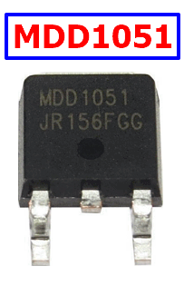
MDD1051 Datasheet PDF – 150V, 28A, N-Channel MOSFET

This is one of the types of MOSFETs and is a kind of transistor.

Part Number: MDD1051

Function: 150V, 28A, N-channel MOSFET

Package: D-PAK ( TO-252 ) Type

Manufacturer: MagnaChip Semiconductor

Image

MDD1051 mosfet datasheet

Description

The MDD1051 uses advanced MagnaChip’s MOSFET Technology, which provides high performance in on-state resistance, fast switching performance and excellent quality. MDD1051 is suitable device for Synchronous Rectification For Server and general purpose applications.

Pinouts:

MDD1051 transistor pinout

Features

1. VDS = 150V

2. ID = 28A @VGS = 10V

3. RDS(ON) (MAX) < 46.0mΩ @VGS = 10V

4. 100% UIL Tested

5. 100% Rg Tested

Absolute Maximum Ratings (Tc = 25°C) :

1. Drain to source voltage: VDSS = 150 V

2. Gate to source voltage: VGSS = ± 20 V

3. Drain current: ID = 28 A

4. Drain power dissipation : PD = 70 W

5. Single pulse avalanche energy : Eas = 50 mJ

6. Channel temperature: Tch = -55 to +150 °C

7. Storage temperature: Tstg = -55 to +150 °C

Other data sheets are available within the file: MDD-1051

MDD1051 Datasheet PDF Download


MDD1051 pdf

Related articles across the web