C5198 Transistor – NPN Transisor, 140V, 10A, 2SC5198

C5198 is Silicon NPN Triple Diffused Type Transistor.

Part Number: 2SC5198

Function: NPN Transisor, 140V, 10A

Package: TO-3PN Type

Manufacturer: Toshiba

Image:

C5198 datasheet


Description

C5198 is a type of bipolar junction transistor (BJT) made from silicon, a semiconductor material. This transistor is designed for amplifying or switching electronic signals in various electronic circuits. It is often paired with its complementary PNP transistor 2SA1941. It’s widely used in high-quality audio amplifiers because of its robust power handling, low distortion, and good linearity.


Features

1.  High breakdown voltage: VCEO= 140 V (min)

2. Complementary to 2SA1941

3. Suitable for use in 70-W high fidelity audio amplifier’s output stage


Electrical Characteristics (Ta = 25°C)
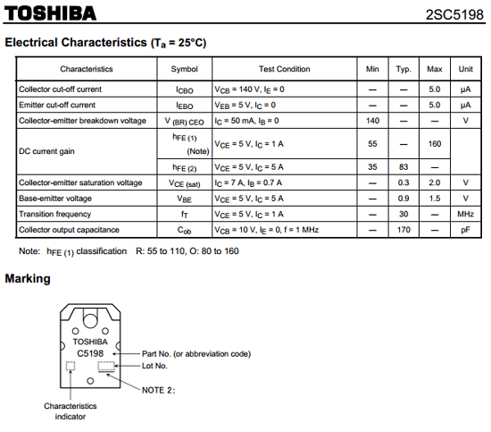
components


Absolute Maximum Ratings (Ta= 25°C)

1. Collector-base voltage : VCBO = 140 V

2. Collector-emitter voltage : VCEO = 140 V

3. Emitter-base voltage : VEBO = 5 V

4. Collector current : IC = 10 A

5. Base current : IB = 1 A

6. Collector power dissipation  (Tc= 25°C) : PC = 100 W

7. Junction temperature : Tj  = 150 °C


Applications

1. Audio power amplifier output stages

2. Power supply regulation and switching


Equivalent & Alternative Parts

1. 2SA1941 (PNP) – Complementary partner for push-pull audio stages

2. 2SC5200 (NPN) – Similar high-power audio transistor (VCEO 230 V, 15 A)

3. MJ21194 (NPN) – Audio power transistor with higher current (VCEO 250 V, 16 A)


Other data sheets are available within the file:  2SC5198


C5198 Datasheet Download


C5198 pdf

Posts related to ‘ 2SC ~ ‘

Part number Description
2SC2482 300V, Silicon NPN Transistor – Toshiba
2SC2625 400V, 10A, NPN Power Transistor
2SC2655 50V, 2A, NPN Amplifier Transistor
2SC2482 Toshiba Transistor ( NPN, Transistor )
2SC2500 2SC2500 Transistor – 10V, 2A, NPN ( Datasheet PDF )
2SC4520 2SC4520 Transistor – 45V, 1.5A, NPN ( Datasheet PDF )
2SC3552 500V, 12A, NPN Transistor
2SC4942 600V, 1A, NPN Transistor – NEC
2SC2610 2SC2610 Transistor – 300V, 100mA, NPN ( Datasheet PDF )
2SC4424 2SC4424 Transistor – 400V, 16A, NPN ( Datasheet PDF )


HEF4007UBP Datasheet – Dual Complementary Pair and Inverter

Dual Complementary Pair and Inverter is an electronic structure that includes two comparative and opposing corpora and an inverter.

Part Number: HEF4007UB

Function: Dual Complementary Pair and Inverter

Package: DIP 14 Pin type

Manufacturer: Philips Semiconductor, NXP

Image


Description

The HEF4007UBP is a dual complementary pair and an inverter with access to each device. It has three n-channel and three p-channel enhancement mode MOS transistors.

It has three n-channel and three p-channel enhancement mode MOS transistors. It operates over a recommended VDD power supply range of 3 V to 15 V referenced to VSS (usually ground). Unused inputs must be connected to VDD, VSS, or another input.

Dual Complementary Pair

This includes two complementary MOSFET pairs. These pairs consist of one N-channel MOSFET and one P-channel MOSFET. This dual complementary pair can be used in a variety of applications, including analog switching, digital logic implementation, and signal processing.

Inverter

This IC includes a single inverter. An inverter is a digital circuit element that inverts an input signal. For example, if the input is a logical ‘1’, the output will be a logical ‘0’, and vice versa.


Features

• Fully static operation

• 5 V, 10 V, and 15 V parametric ratings

• Standardized symmetrical output characteristics

• Specified from -40 °C to +85 °C

• Complies with JEDEC standard JESD 13-B

• Inputs and outputs are protected against electrostatic effects

This part has an extended mode MOS characteristic characteristic of three n-content and three p-content, and the recommended V_DD power supply range is defined as 3 V to 15 V relative to V_SS (usually called support). Random user inputs should be connected to V_DD, V_SS or other inputs.

Pinouts

1. SP2, SP3: source connections to 2nd and 3rd p-channel transistors

2. DP1, DP2: drain connections from the 1st and 2nd p-channel transistors

3. DN1, DN2 drain connections from the 1st and 2nd n-channel transistors

4. SN2, SN3 source connections to the 2nd and 3rd n-channel transistors

5. DN/P3 common connection to the 3rd p-channel and n-channel transistor drains

6. G1 to G3 gate connections to n-channel and p-channel of the three transistor pairs


Applications

· High input impedance amplifiers

· Linear amplifiers

· (Crystal) oscillators

· High-current sink and source drivers

· High impedance buffers.

By integrating the dual complementary pair and inverter into a single chip, design flexibility and space efficiency can be maximized.

Other data sheets within the file: HEF4007UB, HEF4007UBD, HEF4007UBT


HEF4007UBP Datasheet PDF

HEF4007UBF pdf

List of search results related to this post

Part number Description
HEF4017B 5-Stage Johnson Decade Counter
HEF4585B 4-bit Magnitude Comparator
HEF4093B Quad 2-Input NAND Schmitt Trigger
HEF4051B 8-Ch, Analog Multiplexer/Demultiplexer
HEF4528B Dual Monostable Multivibrator
HEF4053BT Multiplexer / Demultiplexer – Philips