60R360P Datasheet PDF – 600V, N-ch, MOSFET – Magnachip

Part Number: MMP60R360P, Marking : 60R360P

Function: 600V, 11A, 0.36Ω, N-channel MOSFET

Package: TO-220 Type

Manufacturer: MagnaChip Semiconductor

Image

60R360P pinout datasheet mosfet

Description

The 60R360P is power MOSFET using magnachip’s advanced super junction technology that can realize very low on-resistance and gate charge. It will provide much high efficiency by using optimized charge coupling technology.

These user friendly devices give an advantage of Low EMI to designers as well as low switching loss.

Features

1. Low Power Loss by High Speed Switching and Low On-Resistance

2. 100% Avalanche Tested

3. Green Package – Pb Free Plating, Halogen Free

Applications

1. PFC Power Supply Stages

2. Switching Applications

3. Adapter

4. Motor Control

5. DC – DC Converters


60R360P Datasheet PDF


Posts related to ‘ MOSFET ‘

Part number Description
P6NK60ZFP N-ch, 600V, 6A, MOSFET – ST
K2401 200V, 15A, N-ch MOSFET – Toshiba
70T03GH 30V, 60A, N-Ch, Power MOSFET
2SK3639 20V, 64A, N-Ch, MOSFET – NEC
W60N10 100V, 60A, N-Ch, MOSFET – ST
5R380CE N-Ch, 550V, MOSFET
K3683 500V, MOSFET, 2SK3683 ( PDF ) – Fuji
K1158 N-Ch, 500V, 7A, MOSFET, Transistor
2SJ506 P-Ch, 30V, 10A, MOSFET, Transistor
P70N02LDG 25V, MOSFET – NIKO-SEM ( PDF )


Related articles across the web

PCF0700P/051 PDF – CMOS Gate Arrays, DIP 40, Philips

CMOS gate arrays, also known as CMOS gate array devices, are a type of integrated circuit (IC) that is designed to be customized by the end user for a specific application. They belong to the family of programmable logic devices (PLDs) and are based on complementary metal-oxide-semiconductor (CMOS) technology.

Part Number: PCF0700P/051

Function: CMOS Gate Arrays

Package: DIP 40 Pin Type

Manufacturer: Mullard, Philips

Images:

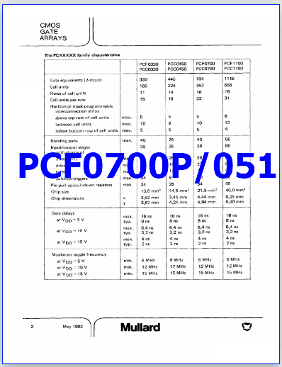
PCF0700P-051 pdf datasheet

Description

The PCF0700P/051 gate array family offers the circuit designer the facility to create a semi-coustom circuit with a unique set of CAD ( Computer-Aided Design ) tools in a well established CMOS process.

The basis for the design procedure is formed by a logic network description, which outlines the required logic in terms of basic functions. A simulation control language offers the ability to verify the logic, simulate it with the actual propagation delay times and generate the test patterns.

PCF0700P_051 pdf array

Here’s how CMOS gate arrays work and what they are used for:

1. Basic Structure: A CMOS gate array consists of a grid of programmable logic cells, also known as “macrocells.” Each macrocell contains a set of basic logic gates (AND, OR, NOT, etc.) that can be interconnected and programmed to perform specific logic functions.

2. Customization: The user designs their desired digital logic circuit by configuring the interconnections between the macrocells using a process known as “mask programming.” This is typically done through software tools provided by the manufacturer. The configured design is then used to generate a custom mask that defines the wiring of the logic cells.

Features

1. Fast development time

2. Low-power CMOS technology

PCF0700P_051 datasheet


PCF0700P/051 Datasheet