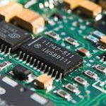
This post explains for the Power Controller.
The Part Number is DK112.
The function of this semiconductor is switching power supply control chip.
The package is DIP-8 Pin Type.
Manufacturer: Dongke semiconductor ( http://www.dkpower.cn/ )
Preview images :

Description
The DK112 is specially design for low power switch mode control, it is widely use in small household electrical appliances. A Switch Mode Power Controller (SMPC) is a type of electronic device or integrated circuit that is used to control and regulate the operation of a switch-mode power supply (SMPS). Switch-mode power supplies are commonly used in a wide range of electronic devices, including computers, mobile phones, LED drivers, and many other applications where efficient voltage regulation and power conversion are required.
Features
1. 65KHz Oscillation Frequency.
2. Double chip design with Bipolar Junction Transistor (BJT) to save cost.
3. Large scale MOS digital circuit design with E pole BJT driving, so that to enhance its High Voltage Resistance capability.
4. Self-power supply design, no need for additional IC to supply the electricity.
5. Internal integrated constant high voltage current driving circuit, no need for additional resistance.
6. Over current, Over loading, Over temperature, Over voltage, Output short circuit and photo-coupler Failure Protection
Pinouts

Applications:
1. Battery charger
2. DVD/VCD power supply
3. Power AC/DC adapters
4. Air conditioner power supply
5. STB power supply
6. AC/DC LED driver applications
7. Electromagnetic oven power supply
8. TV/Monitor power supply
[…]
Note ]
When power on, high voltage AC current transferred to pin of COLLECTOR (pin 5,6,7,8) through
switching transformer. Then it is transferred to transistor’s (Q1 in Start up principle diagram) B pole via internal high voltage constant current driving circuit. The amplified current (about 20 times amplified by transistor Q1) enters power management circuit, charges the VCC external capacitor C1 via D1, and supply a spare voltage of 3.6V for Fb (Fb PIN to ground should be connected with a filter capacitor). When VCC voltage comes up to 5V, oscillator begins to work and controller offers a 25uA ground connecting power for Fb, the circuit enters into normal working mode.
DK112 PDF Datasheet